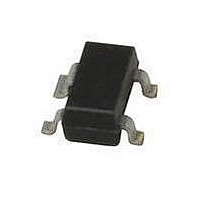
BF1105,215 NXP Semiconductors, BF1105,215 Datasheet - Page 4

BF1105,215
Manufacturer Part Number
BF1105,215
Description
MOSFET N-CH 7V DUAL SOT143
Manufacturer
NXP Semiconductors
Datasheet
1.BF1105R215.pdf
(15 pages)
Specifications of BF1105,215
Package / Case
SOT-143, SOT-143B, TO-253AA
Current Rating
30mA
Frequency
800MHz
Gain
38dB
Transistor Type
N-Channel Dual Gate
Noise Figure
1.7dB
Voltage - Test
5V
Configuration
Dual
Transistor Polarity
Dual N-Channel
Drain-source Breakdown Voltage
7 V
Continuous Drain Current
30 mA
Power Dissipation
200 mW
Mounting Style
SMD/SMT
Lead Free Status / RoHS Status
Lead free / RoHS Compliant
Power - Output
-
Current - Test
-
Lead Free Status / RoHS Status
Lead free / RoHS Compliant, Lead free / RoHS Compliant
NXP Semiconductors
THERMAL CHARACTERISTICS
Note
1. Device mounted on a printed-circuit board.
STATIC CHARACTERISTICS
T
DYNAMIC CHARACTERISTICS
Common source; T
1997 Dec 02
R
R
V
V
V
V
I
I
I
y
C
C
C
C
F
G
X
SYMBOL
SYMBOL
SYMBOL
j
DSX
G1-SS
G2-SS
= 25 C unless otherwise specified.
(BR)DSS
(BR)G1-SS
(BR)G2-SS
G2-S (th)
mod
N-channel dual-gate MOS-FETs
th j-a
th j-s
ig1-ss
ig2-ss
oss
rss
p
fs
thermal resistance from junction to ambient in free air
thermal resistance from junction to soldering point
drain-source breakdown voltage
gate 1-source breakdown voltage V
gate 2-source breakdown voltage V
gate 2-source threshold voltage
self-biasing drain current
gate 1 cut-off current
gate 2 cut-off current
forward transfer admittance
input capacitance at gate 1
input capacitance at gate 2
output capacitance
reverse transfer capacitance f = 1 MHz
noise figure
power gain
cross-modulation
amb
PARAMETER
PARAMETER
= 25 C; V
PARAMETER
G2-S
= 4 V; V
pulsed; T
f = 1 MHz
f = 1 MHz
f = 1 MHz
f = 800 MHz; Y
G
B
G
B
input level for k = 1% at 0 dB AGC;
f
input level for k = 1% at 40 dB AGC;
f
w
w
L
L
S
S
= 50 MHz; f
= 50 MHz; f
= B
= B
DS
= 2 mS; B
= 3.3 mS; B
V
V
V
V
V
= 5 V; self-biasing current; unless otherwise specified.
L opt
L opt
G1-S
G2-S
G1-S
G1-S
G2-S
G1-S
G1-S
j
= 25 C
; f = 200 MHz; see Fig.16
; f = 800 MHz; see Fig.17
= V
= 0; I
= V
= 5 V; V
= 4 V; V
= 5 V; V
= V
CONDITIONS
S
unw
unw
G2-S
DS
DS
S
= B
S
4
CONDITIONS
D
= Y
= B
= 0; I
= 0; V
= 60 MHz; see Fig.18
= 60 MHz; see Fig.18
= 0; I
S opt
DS
DS
G2-S
= 0; I
S opt
S opt
= 5 V; I
= 5 V
G2-S
; G
G1-S
G2-S
= 0; I
D
; G
note 1
L
BF1105; BF1105R; BF1105WR
= 10 A
= 10 A
= 0.5 mS;
L
= 10 A
= 4 V
D
= 1 mS;
D
CONDITIONS
= 0
= 20 A
7
7
7
0.3
8
25
85
100
MIN.
MIN.
0.8
31
2.2
1.6
1.2
25
1.7
38
20
TYP.
TYP.
VALUE
Product specification
350
200
2.7
40
2.5
1.2
16
50
20
MAX.
MAX.
UNIT
K/W
K/W
V
V
V
V
mA
nA
nA
mS
pF
pF
pF
fF
dB
dB
dB
dBV
dBV
UNIT
UNIT


