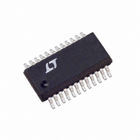
LT5500EGN Linear Technology, LT5500EGN Datasheet - Page 9

LT5500EGN
Manufacturer Part Number
LT5500EGN
Description
IC RECEIVER FRONT END 24-SSOP
Manufacturer
Linear Technology
Datasheet
1.LT5500EGN.pdf
(12 pages)
Specifications of LT5500EGN
Frequency
1.8GHz ~ 2.7GHz
Applications
HS Wireless LAN, Wireless Local Loop
Current - Receiving
23mA
Data Interface
PCB, Surface Mount
Antenna Connector
PCB, Surface Mount
Voltage - Supply
1.8 V ~ 5.25 V
Operating Temperature
-40°C ~ 85°C
Package / Case
24-SSOP
Pin Count
24
Screening Level
Industrial
Lead Free Status / RoHS Status
Contains lead / RoHS non-compliant
Features
-
Sensitivity
-
Memory Size
-
Data Rate - Maximum
-
Modulation Or Protocol
-
Lead Free Status / Rohs Status
Not Compliant
Available stocks
Company
Part Number
Manufacturer
Quantity
Price
Company:
Part Number:
LT5500EGN
Manufacturer:
LT
Quantity:
5 549
Part Number:
LT5500EGN
Manufacturer:
LINEAR/凌特
Quantity:
20 000
Part Number:
LT5500EGN#PBF
Manufacturer:
LINEAR/凌特
Quantity:
20 000
Part Number:
LT5500EGN#TRPBF
Manufacturer:
LINEAR/凌特
Quantity:
20 000
APPLICATIONS
Modes of Operation
The LT5500 has three operating modes:
1. Shutdown
2. LNA High Gain
3. LNA Low Gain
For shutdown, the EN pin and the GS pin must be at logic
Low. Logic Low is defined as a control voltage below 0.3V.
LNA High gain mode requires that both EN and GS pins be
at logic High. Logic High is defined as a control voltage
above 1.35V. LNA Low gain mode requires that the EN pin
be at logic High and that the GS pin be at logic Low. Mixer
operation is independent of the GS pin. The Mixer is
enabled when the EN pin is at logic High.
Table 1: Mode Selection
Evaluation Board
Figure 6 shows the circuit schematic of the evaluation
board. Each signal terminal of the evaluation board has
provisions for three matching components in a T-forma-
tion. In practice, two or fewer components are needed to
achieve the match. In the case of the LNA input, no external
components are necessary if the band select filter pro-
vides the necessary AC coupling. Otherwise AC coupling
must be provided. A similar consideration applies to the
Mixer input pin. The LO terminal of the evaluation board
was designed to permit evaluation of both single ended
and differential matching configurations. The differential
configuration anticipates the use of a transformer. Simi-
larly, the IF output board layout was designed to permit
High
High
Low
EN
High
Low
Low
GS
U
INFORMATION
U
Shutdown
High Gain
Low Gain
LNA
W
Shutdown
MIXER
U
On
On
evaluation of both transformer based and discrete compo-
nent based matching.
The evaluation board employs primarily 0402 surface
mount components, particularly near the signal paths. All
surface mount inductors must have a high self-resonance
frequency. The component values necessary for 1.8GHz
and 2.5GHz applications are tabulated in Figure 3.
RF Layout Tips
• Use 50Ω impedance transmission lines up to the match-
• Keep the matching networks as close to the pins as
• Surface mount 0402 outline (or smaller) parts are
• Improve LO isolation and maximize component density
• Place bypass capacitors to ground in close proximity to
• V
• Avoid use of long traces whenever possible. Long RF
ing networks. Use of ground planes is a must, particu-
larly beneath the IC.
possible.
recommended to minimize parasitic capacitances and
inductances.
by putting the LO signal trace on the bottom of the
board. This permits either the matching components or
an interstage filter to be placed directly between the
LNA output and the Mixer input.
the pull-up inductors on the LNA and Mixer outputs to
improve component behavior and assure a good small-
signal ground.
broadband capacitors to prevent instability. The capaci-
tors should be placed as close as possible to the V
pins.
traces in particular lead to signal radiation, degraded
isolation and higher losses.
CC
lines must be decoupled with low impedance,
LT5500
9
5500f
CC


