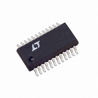
LT5500EGN Linear Technology, LT5500EGN Datasheet - Page 7

LT5500EGN
Manufacturer Part Number
LT5500EGN
Description
IC RECEIVER FRONT END 24-SSOP
Manufacturer
Linear Technology
Datasheet
1.LT5500EGN.pdf
(12 pages)
Specifications of LT5500EGN
Frequency
1.8GHz ~ 2.7GHz
Applications
HS Wireless LAN, Wireless Local Loop
Current - Receiving
23mA
Data Interface
PCB, Surface Mount
Antenna Connector
PCB, Surface Mount
Voltage - Supply
1.8 V ~ 5.25 V
Operating Temperature
-40°C ~ 85°C
Package / Case
24-SSOP
Pin Count
24
Screening Level
Industrial
Lead Free Status / RoHS Status
Contains lead / RoHS non-compliant
Features
-
Sensitivity
-
Memory Size
-
Data Rate - Maximum
-
Modulation Or Protocol
-
Lead Free Status / Rohs Status
Not Compliant
Available stocks
Company
Part Number
Manufacturer
Quantity
Price
Company:
Part Number:
LT5500EGN
Manufacturer:
LT
Quantity:
5 549
Part Number:
LT5500EGN
Manufacturer:
LINEAR/凌特
Quantity:
20 000
Part Number:
LT5500EGN#PBF
Manufacturer:
LINEAR/凌特
Quantity:
20 000
Part Number:
LT5500EGN#TRPBF
Manufacturer:
LINEAR/凌特
Quantity:
20 000
APPLICATIONS
BLOCK DIAGRA
The LT5500 consists of an LNA, a Mixer, an LO buffer and
the associated bias circuitry. The chip is designed to be
compatible with IEEE802.11b wireless local area network
(WLAN), MMDS and other wireless applications. The LNA
and Mixer are designed to operate over an input frequency
range of 1.8GHz to 2.7GHz with a supply voltage of 1.8V
to 5.25V. The Mixer IF output frequency range is typically
10MHz to 450MHz with proper matching. The typical LO
drive is –10dBm. The LO buffer operation is broadband.
LNA
The LNA has two modes of operation: high gain and low
gain. In the high gain mode, the LNA is a cascode
amplifier. Package inductance is used to achieve better
than 10dB input return loss over the entire frequency
range. The input of the LNA must be AC coupled. The
linearity of the high gain mode of the LNA can be in-
creased by adding inductance to LNA_GND. This will
reduce the gain and improve input return loss while
having little impact on the low gain mode. In low gain
mode, the LNA uses a capacitively coupled diode and a
resistively degenerated cascode to attenuate the incom-
ing signal and maintain a moderate VSWR. The LNA
output is an open collector, and the matching circuit
U
INFORMATION
U
W
4, 11, 14, 16, 20, 23
W
2, 9, 17, 21
Figure 2. LT5500 Block Diagram
10
1
3
5
6
7
8
U
EN
V
MIX_GND
LNA_IN
GND
LNA_GND
CC
BIAS
IF
12
LT5500
+
LO
IF
RF
requires a shunt inductor connected to the power supply
to provide the bias current. The component configuration
for matching and example component values are listed in
Figure 3. If it is desirable to reduce the gain further and
simultaneously broaden the LNA bandwidth, an addi-
tional shunt resistor to the power supply can be added to
the output to reduce the output quality factor (Q).
The LT5500 is designed to allow an interstage bandpass
filter to be introduced between the output of the LNA and
the input of the Mixer. If such an interstage filter is
unnecessary, the output of the LNA can be connected to
the Mixer input through a blocking capacitor and small
value resistor.
Mixer
The Mixer consists of a single-ended input differential pair
followed by a double-balanced mixer cell. The input match-
ing configuration for the Mixer is shown in Figure 3. The
Mixer uses a 4.7nH external inductance to act as a high
frequency current source at the MIX_GND pin. Example
component values for matching the mixer input are tabu-
lated in Figure 3.
IF
13
LNA_OUT
–
MIX_IN
LO
LO
GS
–
+
24
22
19
18
15
5500 BD
LT5500
7
5500f


