SAA6588/V2,112 NXP Semiconductors, SAA6588/V2,112 Datasheet - Page 11
SAA6588/V2,112
Manufacturer Part Number
SAA6588/V2,112
Description
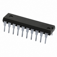
IC RDS/RBDS PRE-PROCESSOR 20DIP
Manufacturer
NXP Semiconductors
Datasheet
1.SAA6588TV2H518.pdf
(32 pages)
Specifications of SAA6588/V2,112
Function
Pre-Processor
Frequency
57kHz
Package / Case
20-DIP (0.300", 7.62mm)
Lead Free Status / RoHS Status
Lead free / RoHS Compliant
Other names
935261513112
SAA6588N
SAA6588N
SAA6588N
SAA6588N


Philips Semiconductors
The transfer of requested data to the main controller is
synchronized via the additional data available output
signal DAVN to avoid loss of RDS/RBDS data. The DAVN
signal is activated if the pre-processor has provided new
data information for the main controller (see Section
“RDS/RBDS data output”) and can be used for the polling
mode as well as for the interrupt mode of the main
microcontroller.
I
The I
pre-processor via internal registers (byte oriented). Those
can either be written by the pre-processor control and read
by the main controller I
The device provides 3 input control registers to which may
be written via the I
may be read via the I
The decoder control updates the output registers after the
detection of a new RDS/RBDS information block and
reads the new mode control settings of the input control
registers. Both operations may occur in the same time slot,
provided that the read operation is complete before a new
RDS/RBDS data bit is processed by the demodulator.
For the corresponding access the registers are addressed
by two separate register pointers, write-enable and
read-enable signals, which are activated either via the
decoder control or via the I
During a read or write transmission from the I
read/write pointer selects the register of the first byte for
transmission and is auto-incremented by the I
control for the transfer of subsequent bytes.
During a write transmission after reception of the device
slave address and write bit, the mode control settings for
the pre-processor have to be send in the protocol
sequence as shown in Table 1 and Fig.5.
During a read cycle after reception of the device slave
address and read bit the requested RDS/RBDS data has
to be received in the protocol sequence as given in Table 2
and Fig.7.
2002 Jan 14
2
C-
RDS/RBDS pre-processor
BUS INTERFACE REGISTERS
2
C-bus interface is connected to other blocks of the
2
C-bus and 7 output registers which
2
C-bus.
2
C-bus or vice versa.
2
C-bus interface control.
2
2
C-bus the
C-bus
11
Table 1 Input control registers
Table 2 Output registers
W
Table 3 Description of initialization and mode control
Byte 0
Byte 1
Byte 2
Byte 0
Byte 1
Byte 2
Byte 3
Byte 4
Byte 5
Byte 6
BIT NAME
7
6
5
4
3
2
1
0
RITE TRANSMISSION FORMAT
DATA
DATA
SQCM 0: triggered signal quality measurement
NWSY 0: normal processing mode
TSQD 0: no determination of signal quality
RBDS 0: RDS processing mode
SYM1 selection of error correction mode for
SYM0
DAC1 selection of data output protocol and
DAC0
W
W
W
R
R
R
R
R
R
R
byte (byte 0
initialization and mode control setting;
see Table 3
pause level and flywheel setting;
see Table 6
pause time/oscillator frequency and
quality detector sensitivity setting;
see Table 7
decoder and data status information;
see Table 12
last processed block (HIGH byte);
see Table 15
last processed block (LOW byte);
see Table 15
previously processed block (HIGH byte);
see Table 15
previously processed block (LOW byte);
see Table 15
error status information; see Table 15
signal quality indication; see Table 15
1: signal quality continuous measurement
1: trigger of signal quality detector
measurement
1: restart of synchronization
synchronization search; see Table 4
1: RBDS processing mode
indirectly control of data available output
signal (DAVN); see Table 5
W
)
FUNCTION
FUNCTION
FUNCTION
Product specification
SAA6588
Related parts for SAA6588/V2,112
Image
Part Number
Description
Manufacturer
Datasheet
Request
R

Part Number:
Description:
Manufacturer:
NXP Semiconductors
Datasheet:
Part Number:
Description:
NXP Semiconductors designed the LPC2420/2460 microcontroller around a 16-bit/32-bitARM7TDMI-S CPU core with real-time debug interfaces that include both JTAG andembedded trace
Manufacturer:
NXP Semiconductors
Datasheet:

Part Number:
Description:
NXP Semiconductors designed the LPC2458 microcontroller around a 16-bit/32-bitARM7TDMI-S CPU core with real-time debug interfaces that include both JTAG andembedded trace
Manufacturer:
NXP Semiconductors
Datasheet:
Part Number:
Description:
NXP Semiconductors designed the LPC2468 microcontroller around a 16-bit/32-bitARM7TDMI-S CPU core with real-time debug interfaces that include both JTAG andembedded trace
Manufacturer:
NXP Semiconductors
Datasheet:
Part Number:
Description:
NXP Semiconductors designed the LPC2470 microcontroller, powered by theARM7TDMI-S core, to be a highly integrated microcontroller for a wide range ofapplications that require advanced communications and high quality graphic displays
Manufacturer:
NXP Semiconductors
Datasheet:
Part Number:
Description:
NXP Semiconductors designed the LPC2478 microcontroller, powered by theARM7TDMI-S core, to be a highly integrated microcontroller for a wide range ofapplications that require advanced communications and high quality graphic displays
Manufacturer:
NXP Semiconductors
Datasheet:
Part Number:
Description:
The Philips Semiconductors XA (eXtended Architecture) family of 16-bit single-chip microcontrollers is powerful enough to easily handle the requirements of high performance embedded applications, yet inexpensive enough to compete in the market for hi
Manufacturer:
NXP Semiconductors
Datasheet:
Part Number:
Description:
The XA-S3 device is a member of Philips Semiconductors? XA(eXtended Architecture) family of high performance 16-bitsingle-chip microcontrollers
Manufacturer:
NXP Semiconductors
Datasheet:

Part Number:
Description:
The NXP BlueStreak LH75401/LH75411 family consists of two low-cost 16/32-bit System-on-Chip (SoC) devices
Manufacturer:
NXP Semiconductors
Datasheet:
Part Number:
Description:
The NXP LPC3130/3131 combine an 180 MHz ARM926EJ-S CPU core, high-speed USB2
Manufacturer:
NXP Semiconductors
Datasheet:
Part Number:
Description:
The NXP LPC3141 combine a 270 MHz ARM926EJ-S CPU core, High-speed USB 2
Manufacturer:
NXP Semiconductors
Part Number:
Description:
The NXP LPC3143 combine a 270 MHz ARM926EJ-S CPU core, High-speed USB 2
Manufacturer:
NXP Semiconductors

Part Number:
Description:
The NXP LPC3152 combines an 180 MHz ARM926EJ-S CPU core, High-speed USB 2
Manufacturer:
NXP Semiconductors
Part Number:
Description:
The NXP LPC3154 combines an 180 MHz ARM926EJ-S CPU core, High-speed USB 2
Manufacturer:
NXP Semiconductors