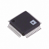
AD9856AST Analog Devices Inc, AD9856AST Datasheet - Page 16

AD9856AST
Manufacturer Part Number
AD9856AST
Description
IC QUADRATURE DGTL UPCONV 48TQFP
Manufacturer
Analog Devices Inc
Series
AD9856r
Datasheet
1.AD9856PCB.pdf
(36 pages)
Specifications of AD9856AST
Rohs Status
RoHS non-compliant
Function
Upconverter
Frequency
5MHz ~ 200MHz
Rf Type
HFC Cable Network
Package / Case
48-LQFP
Available stocks
Company
Part Number
Manufacturer
Quantity
Price
Company:
Part Number:
AD9856AST
Manufacturer:
HOLTEK
Quantity:
40
Company:
Part Number:
AD9856AST
Manufacturer:
AD
Quantity:
1 364
Part Number:
AD9856ASTZ
Manufacturer:
ADI/亚德诺
Quantity:
20 000
AD9856
The sampled carrier is ultimately destined to serve as the input
data to the digital-to-analog converter (DAC) integrated on the
AD9856. The DAC output spectrum is distorted due to the
intrinsic zero-order hold effect associated with DAC-generated
signals. This distortion is deterministic, however, and follows
the familiar SIN(x)/x (or SINC) envelope. Because the SINC
distortion is predictable, it is also correctable—therefore, the
presence of the optional inverse SINC filter preceding the DAC.
This is a FIR filter, which has a transfer function conforming to
the inverse of the SINC response. Thus, when selected, it
modifies the incoming data stream so that the SINC distortion,
which would otherwise appear in the DAC output spectrum, is
virtually eliminated.
As mentioned earlier, the output data is sampled at the rate
of SYSCLK. Because the AD9856 is designed to operate at
SYSCLK frequencies up to 200 MHz, there is the potential
difficulty of trying to provide a stable input clock (REFCLK).
Although stable, commercial high frequency oscillators tend
to be cost prohibitive. To alleviate this problem, the AD9856
has a built-in programmable clock multiplier circuit. This
allows the user to use a relatively low frequency (thus, less
expensive) oscillator to generate the REFCLK signal. The low
frequency REFCLK signal can then be multiplied in frequency
by an integer factor between 4 and 20, inclusive, to become the
SYSCLK signal.
Single-Tone Output Operation
The AD9856 can be configured for frequency synthesis
applications by writing the single-tone bit true. In single-tone
mode, the AD9856 disengages the modulator and preceding
data path logic to output a spectrally pure, single-frequency sine
wave. The AD9856 provides for a 32-bit frequency tuning word,
which results in a tuning resolution of 0.046 Hz at a SYSCLK
rate of 200 MHz.
When using the AD9856 as a frequency synthesizer, a general
rule is to limit the fundamental output frequency to 40% of
SYSCLK. This avoids generating aliases too close to the desired
fundamental output frequency, thus minimizing the cost of
filtering the aliases.
All applicable programming features of the AD9856 apply when
configured in single-tone mode. These features include:
•
•
•
•
Frequency hopping via the profile inputs and associated
tuning word, which allows frequency shift keying (FSK)
modulation.
Ability to bypass the REFCLK multiplier, which results in
lower phase noise and reduced output jitter.
Ability to bypass the SIN(x)/x compensation filter.
Full power-down mode.
Rev. C | Page 16 of 36
INPUT WORD RATE (F
There is a fundamental relationship between the input word
rate (f
source for the AD9856 (REFCLK). The f
at which K-bit data-words (K = 3, 6, or 12) are presented to the
AD9856. However, the following factors affect this relationship:
•
•
•
•
This relationship can be summed as
where H, N, I, and M are integers determined as follows:
H
M
I
N
These conditions show that REFCLK and f
ratio relationship. It is very important that users choose a value
of REFCLK to ensure that this integer ratio relationship is
maintained.
I/Q DATA SYNCHRONIZATION
As mentioned previously, the AD9856 accepts I/Q data pairs
and a twos complement numbering system in three different
word length modes. The full-word mode accepts 12-bit parallel
I and Q data. The half-word mode accepts dual 6-bit I and Q
data inputs to form a 12-bit word. The quarter-word mode
accepts multiple 3-bit I and Q data inputs to form a 12-bit word.
For all word length modes, the AD9856 assembles the data for
signal processing into time-aligned, parallel, 12-bit I/Q pairs.
In addition to the word length flexibility, the AD9856 has
two input timing modes, burst or continuous, that are
programmable via the serial port.
For burst-mode input timing, no external data clock needs to
be provided, because the data is oversampled at the D<11:0>
pins using the system clock (SYSCLK). The TxENABLE pin
is required to frame the data burst, because the rising edge of
TxENABLE is used to synchronize the AD9856 to the input
data rate. The AD9856 registers the input data at the approx-
imate center of the data valid time. Thus, for larger CIC
interpolation rates, more SYSCLK cycles are available to
oversample the input data, maximizing clock jitter tolerances.
The interpolation rate of the CIC filter stage.
Whether or not Half-Band Filter 3 is bypassed.
The value of the REFCLK multiplier (if selected).
Input word length.
REFCLK
=
=
=
=
W
) and the frequency of the clock that serves as the timing
1: Half-Band Filter 3 bypassed
2: Half-Band Filter 3 enabled
1: REFCLK multiplier bypassed
4 ≤ M ≤ 20: REFCLK multiplier enabled
1: Full-word input format
2: Half-word input format
4: Quarter-Word input format
CIC interpolation rate (2 ≤ N ≤ 63)
=
(
2
HNf
W
)
/
MI
W
) vs. REFCLK RELATIONSHIP
W
is defined as the rate
W
have an integer


