0915AT43A0026E Johanson Technology Inc, 0915AT43A0026E Datasheet - Page 10
0915AT43A0026E
Manufacturer Part Number
0915AT43A0026E
Description
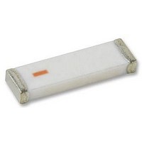
RF CHIP ANTENNA 902 - 928MHZ
Manufacturer
Johanson Technology Inc
Datasheet
1.0783FB15A0100E.pdf
(60 pages)
Specifications of 0915AT43A0026E
Antenna Type
Chip
Number Of Bands
1
Frequency
902MHz ~ 928MHz
Gain
-1dBi
Termination
Surface Mount
Mounting Type
Surface Mount
Impedance
50ohm
Bandwidth
26MHz
Power Rating
2W
Rohs Compliant
Yes
Lead Free Status / RoHS Status
Lead free / RoHS Compliant
Vswr
-
Height (max)
-
Other names
0915AT43A0026
0915AT43A0026
0915AT43A0026E
712-1535-2
Q4586071
0915AT43A0026
0915AT43A0026E
712-1535-2
Q4586071
Available stocks
Company
Part Number
Manufacturer
Quantity
Price


10
D
TEMPERATURE COEFFICIENT:
QUALITY FACTOR / DF:
INSULATION RESISTANCE:
DIELECTRIC STRENGTH:
TEST PARAMETERS:
AVAILABLE CAPACITANCE:
SOLDERABILITY:
RESISTANCE TO
SOLDERING HEAT:
TERMINAL
ADHESION:
PCB DEFLECTION:
LIFE TEST:
THERMAL CYCLE:
HUMIDITY,
STEADY STATE:
HUMIDITY,
LOW VOLTAGE:
VIBRATION:
M
IELECTRIC
ECHANICAL
C
HARACTERISTICS
& E
NVIRONMENTAL
Solder coverage ≥ 90% of metalized areas
No termination degradation
No mechanical damage
Capacitance change: ±2.5% or 0.25pF
Q>500 I.R. >10 G Ohms
Breakdown voltage: 2.5 x WVDC
Termination should not pull off.
Ceramic should remain undamaged.
No mechanical damage.
Capacitance change: 2% or 0.5pF Max
No mechanical damage
Capacitance change: ±3.0% or 0.3 pF
Q>500 I.R. >1 G Ohms
Breakdown voltage: 2.5 x WVDC
No mechanical damage.
Capacitance change: ±2.5% or 0.25pF
Q>2000 I.R. >10 G Ohms
Breakdown voltage: 2.5 x WVDC
No mechanical damage.
Capacitance change: ±5.0% or 0.50pF max.
Q>300 I.R. ≥ 1 G-Ohm
Breakdown voltage: 2.5 x WVDC
No mechanical damage.
Capacitance change: ±5.0% or 0.50pF max.
Q>300 I.R. = 1 G-Ohm min.
Breakdown voltage: 2.5 x WVDC
No mechanical damage.
Capacitance change: ±2.5% or 0.25pF
Q>1000 I.R. ≥ 10 G-Ohm
Breakdown voltage: 2.5 x WVDC
SPECIFICATION
C
0 ± 30ppm /°C, -55 to 125°C
Q
>10 GΩ @ 25°C,WVDC;
125°C IR is 10% of 25°C rating
2.5 X WVDC Min., 25°C, 50 mA max
1MHz ±50kHz, 1.0±0.2 VRMS, 25°C
Size 01005: 0.2 - 10 pF
Size 0201:
Size 0402:
Size 0603:
Size 0805:
Size 1111:
Size 2525:
Size 3838:
HARACTERISTICS
>1,000 @ 1 MHz, Typical 10,000
www.johansontechnology.com
www.johansontechnology.com
NPO
0.2 - 100 pF
0.2 - 33 pF
0.2 - 100 pF
0.3 - 220 pF
0.2 - 1000 pF
1.0 - 2700 pF
1.0 - 5100 pF
Preheat chip to 120°-150°C for 60 sec., dip terminals in rosin flux
then dip in Sn62 solder @ 240°±5°C for 5±1 sec
Preheat device to 80°-100°C for 60 sec.
followed by 150°-180°C for 60 sec.
Dip in 260°±5°C solder for 10±1 sec.
Measure after 24±2 hour cooling period
Linear pull force* exerted on axial leads soldered to each terminal.
Glass epoxy PCB: 0.5 mm deflection
Applied voltage: 200% rated voltage, 50 mA max.
Temperature: 125°±3°C
Test time: 1000+48-0 hours
5 cycles of: 30±3 minutes @ -55°+0/-3°C,
2-3 min. @ 25°C, 30±3 min. @ +125°+3/-0°C,
2-3 min. @ 25°C
Measure after 24±2 hour cooling period
Relative humidity: 90-95%
Temperature: 40°±2°C
Test time: 500 +12/-0 Hours
Measure after 24±2 hour cooling period
Applied voltage: 1.5 VDC, 50 mA max.
Relative humidity: 85±2% Temperature: 40°±2°C
Test time: 240 +12/-0 Hours
Measure after 24±2 hour cooling period
Cycle performed for 2 hours in each of three perpendicular directions
Frequency range 10Hz to 55 Hz to 10 Hz traversed
in 1 minute. Harmonic motion amplitude: 1.5mm
*0402 ≥ 2.0lbs, 0603 ≥ 2.0lbs (min.)
TEST PARAMETERS
± 15%, -55 to 125°C
16VDC DF
10VDC DF
>500 ΩF* or 10 GΩ* @ 25°C,WVDC;
125°C IR is 10% of 25°C rating
* whichever is less
2.5 X WVDC Min., 25°C, 50 mA max
1KHz ±50Hz, 1.0±0.2 VRMS, 25°C
100 - 10,000 pF
≤ 3.5% @ 1 KHz, 25°C
≤ 5.0% @ 1 KHz, 25°C
X7R
Related parts for 0915AT43A0026E
Image
Part Number
Description
Manufacturer
Datasheet
Request
R

Part Number:
Description:
Manufacturer:
Johanson Technology Inc
Datasheet: