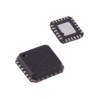
ADL5330ACPZ-R2 Analog Devices Inc, ADL5330ACPZ-R2 Datasheet - Page 5

ADL5330ACPZ-R2
Manufacturer Part Number
ADL5330ACPZ-R2
Description
IC AMP 10MHZ-3GHZ VGA RF 24LFCSP
Manufacturer
Analog Devices Inc
Datasheet
1.ADL5330ACPZ-REEL7.pdf
(24 pages)
Specifications of ADL5330ACPZ-R2
Design Resources
Stable, Closed-Loop Automatic Power Control for RF Appls (CN0050)
Current - Supply
250mA
Frequency
10MHz ~ 3GHz
Gain
10dB
P1db
1.2dBm
Package / Case
24-VFQFN, 24-CSP Exposed Pad
Rf Type
Cellular, CDMA2000, W-CDMA, GSM
Test Frequency
2.7GHz
Voltage - Supply
4.75 V ~ 5.25 V
Lead Free Status / RoHS Status
Lead free / RoHS Compliant
Noise Figure
-
Other names
ADL5330ACPZ-R2TR
ABSOLUTE MAXIMUM RATINGS
Table 2.
Parameter
Supply Voltage VPS1, VPS2
RF Input Power at Maximum Gain
OPHI, OPLO
ENBL
GAIN
Internal Power Dissipation
θ
Maximum Junction Temperature
Operating Temperature Range
Storage Temperature Range
Lead Temperature Range (Soldering 60 sec)
ESD CAUTION
ESD (electrostatic discharge) sensitive device. Electrostatic charges as high as 4000 V readily accumulate on
the human body and test equipment and can discharge without detection. Although this product features
proprietary ESD protection circuitry, permanent damage may occur on devices subjected to high energy
electrostatic discharges. Therefore, proper ESD precautions are recommended to avoid performance
degradation or loss of functionality.
JA
(with Pad Soldered to Board)
Rating
5.5 V
5 dBm at 50 Ω
5.5 V
VPS1, VPS2
2.5 V
1.1 W
60°C/W
150°C
−40°C to +85°C
−65°C to +150°C
300°C
Rev. A | Page 5 of 24
Stresses above those listed under Absolute Maximum Ratings
may cause permanent damage to the device. This is a stress
rating only; functional operation of the device at these or any
other conditions above those indicated in the operational
section of this specification is not implied. Exposure to absolute
maximum rating conditions for extended periods may affect
device reliability.
ADL5330


