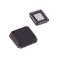
ADL5330ACPZ-R2 Analog Devices Inc, ADL5330ACPZ-R2 Datasheet - Page 13

ADL5330ACPZ-R2
Manufacturer Part Number
ADL5330ACPZ-R2
Description
IC AMP 10MHZ-3GHZ VGA RF 24LFCSP
Manufacturer
Analog Devices Inc
Datasheet
1.ADL5330ACPZ-REEL7.pdf
(24 pages)
Specifications of ADL5330ACPZ-R2
Design Resources
Stable, Closed-Loop Automatic Power Control for RF Appls (CN0050)
Current - Supply
250mA
Frequency
10MHz ~ 3GHz
Gain
10dB
P1db
1.2dBm
Package / Case
24-VFQFN, 24-CSP Exposed Pad
Rf Type
Cellular, CDMA2000, W-CDMA, GSM
Test Frequency
2.7GHz
Voltage - Supply
4.75 V ~ 5.25 V
Lead Free Status / RoHS Status
Lead free / RoHS Compliant
Noise Figure
-
Other names
ADL5330ACPZ-R2TR
APPLICATIONS
BASIC CONNECTIONS
Figure 32 shows the basic connections for operating the
ADL5330. There are two positive supplies, VPS1 and VPS2,
which must be connected to the same potential. Both COM1
and COM2 (common pins) should be connected to a low
impedance ground plane.
A power supply voltage between 4.75 V and 5.25 V should be
applied to VPS1 and VPS2. Decoupling capacitors with 100 pF
and 0.1 μF power supplies should be connected close to each
power supply pin. The VPS2 pins (Pin 18 through Pin 22) can
share a pair of decoupling capacitors because of their proximity
to each other.
The outputs of the ADL5330, OPHI and OPLO, are open
collectors that need to be pulled up to the positive supply with
120 nH RF chokes. The ac-coupling capacitors and the RF
chokes are the principle limitations for operation at low
frequencies. For example, to operate down to 1 MHz, 0.1 μF ac-
coupling capacitors and 1.5 μH RF chokes should be used. Note
that in some circumstances, the use of substantially larger
inductor values results in oscillations.
RF INPUT
VPOS
VPOS
GAIN
0.1μF
C12
0.1μF
C12
100pF
100pF
C13
C14
100pF
C16
100pF
C11
VPS1
COM1
INHI
INLO
COM1
VPS1
C10
1nF
Figure 32. Basic Connections
VPOS
Rev. A | Page 13 of 24
ADL5330
C9
1nF
C2
100pF
C1
0.1μF
Since the differential outputs are biased to the positive supply,
ac-coupling capacitors, preferably 100 pF, are needed between
the ADL5330 outputs and the next stage in the system.
Similarly, the INHI and INLO input pins are at bias voltages of
about 3.3 V above ground.
The nominal input and output impedance looking into each
individual RF input/output pin is 25 Ω. Consequently, the
differential impedance is 50 Ω.
To enable the ADL5330, the ENBL pin must be pulled high.
Taking ENBL low puts the ADL5330 in sleep mode, reducing
current consumption to 250 μA at ambient. The voltage on
ENBL must be greater than 1.7 V to enable the device. When
enabled, the device draws 100 mA at low gain to 215 mA at
maximum gain.
COM2
OPLO
COM2
VPS2
VPS2
OPHI
VPOS
C8
0.1μF
L1
120nH
C7
100pF
VPOS
100pF
100pF
L2
120nH
C5
C6
C4
100pF
C3
0.1μF
RF OUTPUT
ADL5330


