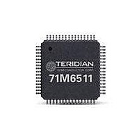
71M6511-IGT/F Maxim Integrated Products, 71M6511-IGT/F Datasheet - Page 45

71M6511-IGT/F
Manufacturer Part Number
71M6511-IGT/F
Description
IC ENERGY METER RESIDENT 64-LQFP
Manufacturer
Maxim Integrated Products
Datasheet
1.71M6511H-IGTF.pdf
(98 pages)
Specifications of 71M6511-IGT/F
Lead Free Status / RoHS Status
Lead free / RoHS Compliant
Available stocks
Company
Part Number
Manufacturer
Quantity
Price
Company:
Part Number:
71M6511-IGT/F
Manufacturer:
ST
Quantity:
1 500
Company:
Part Number:
71M6511-IGT/F
Manufacturer:
Maxim Integrated
Quantity:
10 000
TMUXOUT Pin: One out of 16 digital or 4 analog signals can be selected to be output on the TMUXOUT pin. The function of
the multiplexer is controlled with the I/O RAM register TMUX (0x2000[3:0]), as shown in Table 58.
TMUX[3:0]
Emulator Port: The emulator port, consisting of the pins E_RST, E_TCLK and E_RXTX provides control of the MPU through
an external in-circuit emulator. The emulator port is compatible with the ADM51 emulators manufactured by Signum Systems.
The signals of the emulator port have weak pull-ups. Adding 1kΩ pull-up resistors on the PCB is recommended.
Real-Time Monitor: The RTM output of the CE is available as one of the digital multiplexer options. RTM data is read from the
CE DRAM locations specified by I/O RAM registers RTM0, RTM1, RTM2, and RTM3 after the rise of MUX_SYNC. The RTM can
be enabled and disabled with I/O RAM register RTM_EN. The RTM output is clocked by CKTEST. Each RTM word is clocked
out in 35 cycles and contains a leading flag bit. Figure 13 in the System Timing Section illustrates the RTM output format. RTM
is low when not in use.
SSI Interface: A high-speed serial interface with handshake capability is available to send a contiguous block of CE data to an
external data logger or DSP. The block of data, configurable as to location and size, is sent starting 1 cycle of 32kHz before
each CE code pass begins. If the block of data is big enough that transmission has not completed when the code pass begins,
it will complete during the CE code pass with no timing impact to the CE or the serial data. In this case, care must be taken
that the transmitted data is not modified unexpectedly by the CE. The SSI interface is enabled by the SSI_EN bit and consists
of SCLK, SSDATA, and SFR as outputs and, optionally, SRDY as input. The interface is compatible with 16bit and 32bit
processors. The operation of each pin is as follows:
SCLK is the serial clock. The clock can be 5MHz or 10MHz, as specified by the SSI_10M bit. The SSI_CKGATE bit controls
whether SCLK runs continuously or is gated off when no SSI activity is occurring. If SCLK is gated, it will begin 3 cycles before
SFR rises and will persist 3 cycles after the last data bit is output.
The pins used for the SSI are multiplexed with the LCD segment outputs, as shown in Table 59. Thus, the LCD should be
disabled when the SSI is in use.
Page: 45 of 98
A Maxim Integrated Products Brand
Mode
A
B
C
D
E
0
1
2
3
4
5
6
7
8
9
F
Function
© 2005–2010 Teridian Semiconductor Corporation
analog
analog
analog
analog
digital
digital
digital
digital
digital
digital
digital
digital
digital
digital
digital
--
Table 58: TMUX[3:0] Selections
DGND
IBIAS
PLL_2.5V
VBIAS
RTM (Real time output from CE)
WDTR_EN (Comparator 1 Output AND V1LT3)
reserved
reserved
RXD (from Optical interface)
MUX_SYNC
CK_10M
CK_MPU
reserved for production test
RTCLK
CE_BUSY
XFER_BUSY
Single-Phase Energy Meter IC
71M6511/71M6511H
DATA SHEET
NOVEMBER 2010
V2.7


