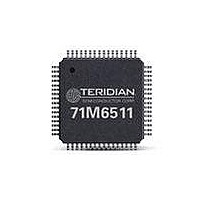
71M6511-IGT/F Maxim Integrated Products, 71M6511-IGT/F Datasheet - Page 39

71M6511-IGT/F
Manufacturer Part Number
71M6511-IGT/F
Description
IC ENERGY METER RESIDENT 64-LQFP
Manufacturer
Maxim Integrated Products
Datasheet
1.71M6511H-IGTF.pdf
(98 pages)
Specifications of 71M6511-IGT/F
Lead Free Status / RoHS Status
Lead free / RoHS Compliant
Available stocks
Company
Part Number
Manufacturer
Quantity
Price
Company:
Part Number:
71M6511-IGT/F
Manufacturer:
ST
Quantity:
1 500
Company:
Part Number:
71M6511-IGT/F
Manufacturer:
Maxim Integrated
Quantity:
10 000
The I/O RAM bit register FLASH66Z defines the pulse width for accessing flash memory. To minimize supply current draw,
this bit should be set to 1.
Flash erasure is initiated by writing a specific data pattern to specific SFR registers in the proper sequence. These special
pattern/sequence requirements prevent inadvertent erasure of the flash memory.
The mass erase sequence is:
The page erase sequence is:
Writing to flash memory:
The MPU may write to the flash memory for non-volatile data storage or when implementing a boot-loader. The I/O RAM
register FLSH_PWE (flash program write enable, SFR B2[0]) differentiates 80515 data store instructions (MOVX@DPTR,A)
between flash and XRAM writes. Before setting FLSH_PWE, all interrupts need to be disabled by setting EAL =1. After the write
operation, FLSH_PWE must be cleared.
The original state of a flash byte is 0xFF (all bits are 1). Overwriting programmed flash cells with a different value usually re-
quires that the cell is erased first. Since cells cannot be erased individually, the page has to be copied to RAM, followed by a
page erase. After this, the page can be updated in RAM and then written back to the flash memory.
excluding the critical addresses from the write operation.
MPU RAM: The 71M6511 includes 2KB of static RAM memory on-chip (XRAM), which are backed-up by the battery plus 256-
bytes of internal RAM in the MPU core. The 2KB of static RAM are used for data storage during normal MPU operations.
CE DRAM: The CE DRAM is the data memory of the CE. The MPU can read and write the CE DRAM as the primary means of
data communication between the two processors.
CE PRAM: The CE PRAM is the program memory of the CE. The CE PRAM has to be loaded with CE code before the CE
starts operating. CE PRAM cannot be accessed by the MPU when the CE is running.
Oscillator
The oscillator drives a standard 32.768kHz watch crystal (see Figure 9). Crystals of this type are accurate and do not require a
high current oscillator circuit. The oscillator in the TERIDIAN 71M6511 Power Meter IC has been designed specifically to
handle watch crystals and is compatible with their high impedance and limited power handling capability. The oscillator power
dissipation is very low to maximize the lifetime of any battery backup device attached to the VBAT pin.
Page: 39 of 98
1.
2.
Note: The mass erase cycle can only be initiated when the ICE port is enabled.
1.
2.
A Maxim Integrated Products Brand
0x07FF (MPU RAM), plus CE DRAM and CE PRAM. It is critical to maintain the integrity of the cells 0x2000…0x2007
as a minimum (where important system settings are stored) during the flash-write operation. This can be achieved by
Writing to flash locations will affect the corresponding XRAM cells, i.e. 0x2000 to 0x20FF (I/O RAM), 0x0000 to
Write 1 to the FLSH_MEEN bit (SFR address 0xB2[1].
Write pattern 0xAA to FLSH_ERASE (SFR address 0x94)
Write the page address to FLSH_PGADR (SFR address 0xB7[7:1]
Write pattern 0x55 to FLSH_ERASE (SFR address 0x94)
© 2005–2010 Teridian Semiconductor Corporation
Single-Phase Energy Meter IC
71M6511/71M6511H
DATA SHEET
NOVEMBER 2010
V2.7


