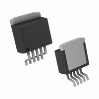
LM9076S-5.0/NOPB National Semiconductor, LM9076S-5.0/NOPB Datasheet - Page 6

LM9076S-5.0/NOPB
Manufacturer Part Number
LM9076S-5.0/NOPB
Description
IC REGULATOR LDO 5V 150MA TO-263
Manufacturer
National Semiconductor
Type
Voltage Regulatorr
Specifications of LM9076S-5.0/NOPB
Regulator Topology
Positive Fixed
Voltage - Output
5V
Voltage - Input
5.35 ~ 40 V
Voltage - Dropout (typical)
0.15V @ 150mA
Number Of Regulators
1
Current - Output
150mA
Operating Temperature
-40°C ~ 125°C
Mounting Type
Surface Mount
Package / Case
TO-263-5, D²Pak (5 leads + Tab), TO-263BA
Current, Output
150 mA
Package Type
TO-263
Regulation, Line
17 mV
Regulation, Load
42 mV
Regulator Type
Low Dropout
Resistance, Thermal, Junction To Case
2.9 °C/W
Temperature, Operating, Range
-40 to +125 °C
Voltage, Dropout
150 mV
Voltage, Input
5.35 to 40 V
Voltage, Output
5 V
Voltage, Supply, Rejection Ratio
60 dB
Lead Free Status / RoHS Status
Lead free / RoHS Compliant
Current - Limit (min)
-
Lead Free Status / Rohs Status
RoHS Compliant part
Electrostatic Device
Other names
*LM9076S-5.0
*LM9076S-5.0/NOPB
LM9076S-5.0
*LM9076S-5.0/NOPB
LM9076S-5.0
Available stocks
Company
Part Number
Manufacturer
Quantity
Price
Part Number:
LM9076S-5.0/NOPB
Manufacturer:
TI/德州仪器
Quantity:
20 000
www.national.com
SHUTDOWN CONTROL LOGIC — LM9076BMA-5.0 Only
Note 1: Absolute Maximum Ratings indicate the limits beyond which the device may cease to function, and/or damage to the device may occur.
Note 2: Operating Ratings indicate conditions for which the device is intended to be functional, but does not guarantee specific performance limits. For guaranteed
specifications and conditions refer to the Electrical Characteristics
Note 3: Not Production tested, Guaranteed by Design. Minimum, Typical, and/or Maximum values are provided for informational purposes only.
Note 4: Pulse testing used maintain constant junction temperature (T
Note 5: The regulated output voltage specification is not guaranteed for the entire range of V
maximum junction temperature (T
output load current. When operating with maximum load currents the input voltage and/or ambient temperature will be limited. When operating with maximum
input voltage the load current and/or the ambient temperature will be limited.
Note 6: Worst case (FREE AIR) per EIA/JESD51–3.
Symbol
V
V
I
t
I
I
DELAY
DELAY
IH(SD)
IL(SD)
V
IH(SD)
IL(SD)
OL
J
C
SHUTDOWN Pin High
SHUTDOWN Pin High
SHUTDOWN Pin Low
SHUTDOWN Pin Low
). The junction temperature is influenced by the ambient temperature (T
DELAY
Threshold Voltage
Threshold Voltage
Reset Delay Time
C
DELAY
Bias Current
Bias Current
Parameter
Current
pin low voltage
Charging
V
V
V
I
V
0.001 uF
V
from V
RESET pin HIGH
V
from 5.0V until V
>4.5V (V
V
from 0V until V
(V
V
V
V
V
SINK
IN
DELAY
OUT
IN
OUT
SHUTDOWN
SHUTDOWN
SHUTDOWN
SHUTDOWN
SHUTDOWN
SHUTDOWN
OUT
J
= 14V,
= 14V, C
).
= I
< 4.0V,
rising from 0V, Δt
= Off)
Conditions
OUT
= 0V
DELAY
OUT
> V
6
pin falling
pin rising
= 40V
= 5V
= 2V
= 0V
DELAY
= On)
OR
OUT
OUT
to
< 0.5V
=
IN
and output loads. Device operational range is limited by the
-0.70
Min
7.1
–
1
–
–
–
–
–
A
), package selection, input voltage (V
0.100
-0.42
11.9
Typ
1.5
1.5
35
15
6
0
-0.25
Max
20.0
35
10
2
–
–
–
–
IN
), and the
Units
uA
ms
μA
μA
μA
μA
V
V
V


