NCV4274AST33T3G ON Semiconductor, NCV4274AST33T3G Datasheet - Page 12
NCV4274AST33T3G
Manufacturer Part Number
NCV4274AST33T3G
Description
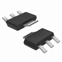
IC REG LDO 400MA 3.3V SOT-223
Manufacturer
ON Semiconductor
Specifications of NCV4274AST33T3G
Regulator Topology
Positive Fixed
Voltage - Output
3.3V
Voltage - Input
4.5 ~ 40 V
Number Of Regulators
1
Current - Output
400mA
Current - Limit (min)
400mA
Operating Temperature
-40°C ~ 150°C
Mounting Type
Surface Mount
Package / Case
SOT-223 (3 leads + Tab), SC-73, TO-261
Number Of Outputs
1
Polarity
Positive
Input Voltage Max
40 V
Output Voltage
3.3 V
Output Type
Fixed
Dropout Voltage (max)
1.23 V @ 250 mA
Output Current
0.4 A
Line Regulation
25 mV
Load Regulation
20 mV
Voltage Regulation Accuracy
2 %
Maximum Operating Temperature
150 C
Mounting Style
SMD/SMT
Minimum Operating Temperature
- 40 C
Lead Free Status / RoHS Status
Lead free / RoHS Compliant
Voltage - Dropout (typical)
-
Lead Free Status / Rohs Status
Lead free / RoHS Compliant
Other names
NCV4274AST33T3G
NCV4274AST33T3GOSTR
NCV4274AST33T3GOSTR
Available stocks
Company
Part Number
Manufacturer
Quantity
Price

Part Number:
NCV4274AST33T3G
Manufacturer:
ON/安森美
Quantity:
20 000


Output Regulator
and error amplifier. The PNP output has saturation control
for regulation while the input voltage is low, preventing over
saturation. Current limit and voltage monitors complement
the regulator design to give safe operating signals to the
processor and control circuits.
Stability Considerations
compensating input line reactance. Possible oscillations
caused by input inductance and input capacitance can be
damped by using a resistor of approximately 1 W in series
with C
three main characteristics of a linear regulator: startup delay,
load transient response and loop stability.
availability, size and temperature constraints. The
aluminum electrolytic capacitor is the least expensive
solution, but, if the circuit operates at low temperatures
(-25°C to -40°C), both the value and ESR of the capacitor
will vary considerably. The capacitor manufacturer's data
sheet usually provides this information.
should work for most applications; however, it is not
necessarily the optimized solution. Stability is guaranteed at
values C
operating temperature range. Actual limits are shown in a
graph in the Typical Performance Characteristics section.
Calculating Power Dissipation in a Single Output
Linear Regulator
regulator (Figure 3) is:
Where:
V
V
I
and
I
Q(max)
q
I(max)
Q(min)
The output is controlled by a precision trimmed reference
The input capacitor C
The output or compensation capacitor helps determine
The capacitor value and type should be based on cost,
The value for the output capacitor C
The maximum power dissipation for a single output
is the quiescent current the regulator consumes at I
I2.
P
is the maximum output current for the application,
is the maximum input voltage,
is the minimum output voltage,
D(max)
Q
w 2.2 mF and an ESR v 2.5 W within the
+ [V
I(max)
* V
I1
in Figure 2 is necessary for
Q(min)
]I
Q(max)
Q
) V
shown in Figure 2
APPLICATION DESCRIPTION
I(max)
NCV4274, NCV4274A
I
q
Q(max)
http://onsemi.com
(eq. 1)
.
12
permissible value of R
package section of the data sheet. Those packages with
R
the die temperature below 150°C. In some cases, none of the
packages will be sufficient to dissipate the heat generated by
the IC, and an external heat sink will be required. The current
flow and voltages are shown in the Measurement Circuit
Diagram.
Heat Sinks
package to improve the flow of heat away from the IC and
into the surrounding air.
outside environment will have a thermal resistance. Like
series electrical resistances, these resistances are summed to
determine the value of R
Where:
R
R
R
R
R
interface between them. These values appear in data sheets
of heat sink manufacturers. Thermal, mounting, and
heat sinking are discussed in the ON Semiconductor
application
ON Semiconductor Website.
qJA
qJC
qCS
qSA
qJC
qSA
Once the value of P
The value of R
A heat sink effectively increases the surface area of the
Each material in the heat flow path between the IC and the
Like R
's less than the calculated value in Equation 2 will keep
= the junction-to-case thermal resistance,
appears in the package section of the data sheet.
= the case-to-heat sink thermal resistance, and
= the heat sink-to-ambient thermal resistance.
are functions of the package type, heat sink and the
P
R
q JA
qJA
qJA
+
+ R
, it too is a function of package type. R
note
150 C * T
qJA
qJC
) R
P
can then be compared with those in the
D
AN1040/D,
qJA
qCS
D(max)
qJA
can be calculated:
A
) R
:
is known, the maximum
qSA
available
on
qCS
(eq. 2)
(eq. 3)
and
the
Related parts for NCV4274AST33T3G
Image
Part Number
Description
Manufacturer
Datasheet
Request
R

Part Number:
Description:
Voltage Regulator Family
Manufacturer:
ON Semiconductor
Datasheet:
Part Number:
Description:
ON Semiconductor [VOLTAGE REGULATOR]
Manufacturer:
ON Semiconductor
Datasheet:
Part Number:
Description:
357-036-542-201 CARDEDGE 36POS DL .156 BLK LOPRO
Manufacturer:
ON Semiconductor
Datasheet:
Part Number:
Description:
357-036-542-201 CARDEDGE 36POS DL .156 BLK LOPRO
Manufacturer:
ON Semiconductor
Datasheet:
Part Number:
Description:
357-036-542-201 CARDEDGE 36POS DL .156 BLK LOPRO
Manufacturer:
ON Semiconductor
Datasheet:
Part Number:
Description:
357-036-542-201 CARDEDGE 36POS DL .156 BLK LOPRO
Manufacturer:
ON Semiconductor
Datasheet:
Part Number:
Description:
357-036-542-201 CARDEDGE 36POS DL .156 BLK LOPRO
Manufacturer:
ON Semiconductor
Datasheet:
Part Number:
Description:
357-036-542-201 CARDEDGE 36POS DL .156 BLK LOPRO
Manufacturer:
ON Semiconductor
Datasheet:
Part Number:
Description:
357-036-542-201 CARDEDGE 36POS DL .156 BLK LOPRO
Manufacturer:
ON Semiconductor
Datasheet:
Part Number:
Description:
357-036-542-201 CARDEDGE 36POS DL .156 BLK LOPRO
Manufacturer:
ON Semiconductor
Datasheet:
Part Number:
Description:
357-036-542-201 CARDEDGE 36POS DL .156 BLK LOPRO
Manufacturer:
ON Semiconductor
Datasheet:
Part Number:
Description:
357-036-542-201 CARDEDGE 36POS DL .156 BLK LOPRO
Manufacturer:
ON Semiconductor
Datasheet:
Part Number:
Description:
Manufacturer:
ON Semiconductor
Datasheet:
Part Number:
Description:
Manufacturer:
ON Semiconductor
Datasheet: