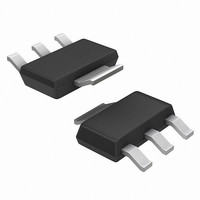
NCV4274AST33T3G ON Semiconductor, NCV4274AST33T3G Datasheet

NCV4274AST33T3G
Specifications of NCV4274AST33T3G
NCV4274AST33T3GOSTR
Available stocks
Related parts for NCV4274AST33T3G
NCV4274AST33T3G Summary of contents
Page 1
NCV4274, NCV4274A 400 mA 2% and 4%Voltage Regulator Family Description The NCV4274 and NCV4274A is a precision micro−power voltage regulator with an output current capability of 400 mA available in the DPAK, D2PAK and SOT−223 packages. The output voltage is ...
Page 2
I Bandgap Refernece Thermal Shutdown Pin Definitions and Functions Pin No. Symbol 1 I Input; Bypass directly at the IC a ceramic capacitor to GND. 2,4 GND Ground 3 Q Output; Bypass with a capacitor to GND. 1. DPAK 3LD ...
Page 3
OPERATING RANGE Parameter Input Voltage (8.5 V Version) Input Voltage (5.0 V Version) Input Voltage (3.3 V, and 2.5 V Version) Junction Temperature THERMAL RESISTANCE Parameter Junction−to−Ambient Junction−to−Ambient Junction−to−Case Junction−to−Case Junction−to−Tab Junction−to−Ambient 4. Soldered in, minimal footprint, FR4 2 5. ...
Page 4
ELECTRICAL CHARACTERISTICS −40°C < T < 150° 13.5 V unless otherwise noted Parameter REGULATOR Output Voltage (8.5 V Version) Output Voltage (8.5 V Version) Output Voltage (5.0 V Version) Output Voltage (5.0 V Version) Output Voltage ...
Page 5
NCV4274 NCV4274A 1.0 mF 100 2,4 GND I GND Figure 2. Measuring Circuit TYPICAL CHARACTERISTIC CURVES 100 10 Maximum ESR − 100 ...
Page 6
TYPICAL CHARACTERISTIC CURVES − 8.5 V Version 8.6 8.5 8.4 8.3 − (°C) J Figure 6. Output Voltage vs. Junction Temperature 1000 T = 25°C ...
Page 7
TYPICAL CHARACTERISTIC CURVES − 8.5 V Version (V) I Figure 12. Current Consumption vs. Input Voltage 6 ...
Page 8
TYPICAL CHARACTERISTIC CURVES − 5.0 V Version 5 13 5.1 5.0 4.9 4.8 − (°C) J Figure 14. Output Voltage vs. Junction Temperature 800 T = 25°C ...
Page 9
TYPICAL CHARACTERISTIC CURVES − 5.0 V Version (V) I Figure 20. Current Consumption vs. Input Voltage 6 ...
Page 10
TYPICAL CHARACTERISTIC CURVES − 3.3 V Version 3 3 3.3 3.2 3.1 3.0 2.9 − (°C) J Figure 22. Output Voltage vs. Junction Temperature 800 T ...
Page 11
TYPICAL CHARACTERISTIC CURVES − 3.3 V Version (V) I Figure 28. Current Consumption vs. Input Voltage 25°C 0 ...
Page 12
TYPICAL CHARACTERISTIC CURVES − 2.5 V Version 2 2 2.5 2.4 2.3 2.2 2.1 − (°C) J Figure 30. Output Voltage vs. Junction Temperature 800 T ...
Page 13
TYPICAL CHARACTERISTIC CURVES − 2.5 V Version 4.5 4.0 3.5 3.0 2.5 2.0 1.5 1.0 0 (V) I Figure 36. Current Consumption vs. Input Voltage ...
Page 14
... Like R qJA R are functions of the package type, heat sink and the qSA interface between them. These values appear in data sheets of heat sink manufacturers. Thermal, mounting, and heat sinking are discussed in the ON Semiconductor application ) Semiconductor Website. (eq I(max) . ...
Page 15
... NCV4274DT50G 4% NCV4274DT50RKG 4% NCV4274ADS50G 2% NCV4274ADS50R4G 2% NCV4274ADT50G 2% NCV4274ADT50RKG 2% NCV4274ST33T3G 4% NCV4274DT33RKG 4% NCV4274AST33T3G 2% NCV4274ADT33RKG 2% NCV4274ST25T3G 4% NCV4274AST25T3G 2% †For information on tape and reel specifications, including part orientation and tape sizes, please refer to our Tape and Reel Packaging Specifications Brochure, BRD8011/D. Output Voltage Package 8.5 V D2PAK (Pb−Free) 8.5 V D2PAK (Pb− ...
Page 16
... A 0.08 (0003) A1 2.0 0.079 *For additional information on our Pb−Free strategy and soldering details, please download the ON Semiconductor Soldering and Mounting Techniques Reference Manual, SOLDERRM/D. PACKAGE DIMENSIONS SOT−223 (TO−261) CASE 318E−04 ISSUE N NOTES: 1. DIMENSIONING AND TOLERANCING PER ASME Y14.5M, 1994. ...
Page 17
... DETAIL 0.005 (0.13 *For additional information on our Pb−Free strategy and soldering details, please download the ON Semiconductor Soldering and Mounting Techniques Reference Manual, SOLDERRM/D. PACKAGE DIMENSIONS DPAK (SINGLE GAUGE) CASE 369C−01 ISSUE GAUGE L2 SEATING C PLANE PLANE DETAIL A ROTATED SOLDERING FOOTPRINT* 6.20 3 ...
Page 18
... *For additional information on our Pb−Free strategy and soldering details, please download the ON Semiconductor Soldering and Mounting Techniques Reference Manual, SOLDERRM/D. ON Semiconductor and are registered trademarks of Semiconductor Components Industries, LLC (SCILLC). SCILLC reserves the right to make changes without further notice to any products herein. SCILLC makes no warranty, representation or guarantee regarding the suitability of its products for any particular purpose, nor does SCILLC assume any liability arising out of the application or use of any product or circuit, and specifically disclaims any and all liability, including without limitation special, consequential or incidental damages. “ ...


