NCV4274AST33T3G ON Semiconductor, NCV4274AST33T3G Datasheet - Page 2
NCV4274AST33T3G
Manufacturer Part Number
NCV4274AST33T3G
Description
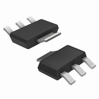
IC REG LDO 400MA 3.3V SOT-223
Manufacturer
ON Semiconductor
Specifications of NCV4274AST33T3G
Regulator Topology
Positive Fixed
Voltage - Output
3.3V
Voltage - Input
4.5 ~ 40 V
Number Of Regulators
1
Current - Output
400mA
Current - Limit (min)
400mA
Operating Temperature
-40°C ~ 150°C
Mounting Type
Surface Mount
Package / Case
SOT-223 (3 leads + Tab), SC-73, TO-261
Number Of Outputs
1
Polarity
Positive
Input Voltage Max
40 V
Output Voltage
3.3 V
Output Type
Fixed
Dropout Voltage (max)
1.23 V @ 250 mA
Output Current
0.4 A
Line Regulation
25 mV
Load Regulation
20 mV
Voltage Regulation Accuracy
2 %
Maximum Operating Temperature
150 C
Mounting Style
SMD/SMT
Minimum Operating Temperature
- 40 C
Lead Free Status / RoHS Status
Lead free / RoHS Compliant
Voltage - Dropout (typical)
-
Lead Free Status / Rohs Status
Lead free / RoHS Compliant
Other names
NCV4274AST33T3G
NCV4274AST33T3GOSTR
NCV4274AST33T3GOSTR
Available stocks
Company
Part Number
Manufacturer
Quantity
Price

Part Number:
NCV4274AST33T3G
Manufacturer:
ON/安森美
Quantity:
20 000


1. DPAK 3LD package code 6025
2. D2PAK 3LD package code 6083
Stresses exceeding Maximum Ratings may damage the device. Maximum Ratings are stress ratings only. Functional operation above the
Recommended Operating Conditions is not implied. Extended exposure to stresses above the Recommended Operating Conditions may affect
device reliability.
3. This device series incorporates ESD protection and is tested by the following methods:
Pin Definitions and Functions
ABSOLUTE MAXIMUM RATINGS
I, Input−to−Regulator
I, Input peak Transient Voltage to Regulator with Respect
to GND
Q, Regulated Output
GND, Ground Current
Junction Temperature
Storage Temperature
ESD Capability, Human Body Model
ESD Capability, Machine Model
ESD Capability, Charged Device Model
Pin No.
ESD HBM tested per AEC−Q100−002 (EIA/JESD22−A114)
ESD MM tested per AEC−Q100−003 (EIA/JESD22−A115)
ESD CDM tested per EIA/JES D22/C101, Field Induced Charge Model
2,4
1
3
Symbol
GND
Pin Symbol, Parameter
Q
I
Input; Bypass directly at the IC a ceramic capacitor to GND.
Ground
Output; Bypass with a capacitor to GND.
I
Refernece
Shutdown
Bandgap
Thermal
Voltage
Current
Voltage
Current
Figure 1. Block Diagram
http://onsemi.com
ESD
Symbol
ESD
ESD
+
I
−
T
GND
V
T
V
V
I
Stg
I
Q
I
Q
J
CDM
I
I
MM
HB
2
Function
Current Limit and
Saturation Sense
Condition
V
Q
=
V
I
Internally
Internally
Limited
Limited
−1.0
Min
−42
−50
200
−
−
4
1
Q
GND
Internally
Internally
Limited
Limited
Max
100
150
150
45
60
40
Unit
mA
kV
kV
°C
°C
V
V
V
V
Related parts for NCV4274AST33T3G
Image
Part Number
Description
Manufacturer
Datasheet
Request
R

Part Number:
Description:
Voltage Regulator Family
Manufacturer:
ON Semiconductor
Datasheet:
Part Number:
Description:
ON Semiconductor [VOLTAGE REGULATOR]
Manufacturer:
ON Semiconductor
Datasheet:
Part Number:
Description:
357-036-542-201 CARDEDGE 36POS DL .156 BLK LOPRO
Manufacturer:
ON Semiconductor
Datasheet:
Part Number:
Description:
357-036-542-201 CARDEDGE 36POS DL .156 BLK LOPRO
Manufacturer:
ON Semiconductor
Datasheet:
Part Number:
Description:
357-036-542-201 CARDEDGE 36POS DL .156 BLK LOPRO
Manufacturer:
ON Semiconductor
Datasheet:
Part Number:
Description:
357-036-542-201 CARDEDGE 36POS DL .156 BLK LOPRO
Manufacturer:
ON Semiconductor
Datasheet:
Part Number:
Description:
357-036-542-201 CARDEDGE 36POS DL .156 BLK LOPRO
Manufacturer:
ON Semiconductor
Datasheet:
Part Number:
Description:
357-036-542-201 CARDEDGE 36POS DL .156 BLK LOPRO
Manufacturer:
ON Semiconductor
Datasheet:
Part Number:
Description:
357-036-542-201 CARDEDGE 36POS DL .156 BLK LOPRO
Manufacturer:
ON Semiconductor
Datasheet:
Part Number:
Description:
357-036-542-201 CARDEDGE 36POS DL .156 BLK LOPRO
Manufacturer:
ON Semiconductor
Datasheet:
Part Number:
Description:
357-036-542-201 CARDEDGE 36POS DL .156 BLK LOPRO
Manufacturer:
ON Semiconductor
Datasheet:
Part Number:
Description:
357-036-542-201 CARDEDGE 36POS DL .156 BLK LOPRO
Manufacturer:
ON Semiconductor
Datasheet:
Part Number:
Description:
Manufacturer:
ON Semiconductor
Datasheet:
Part Number:
Description:
Manufacturer:
ON Semiconductor
Datasheet: