AD713JN Analog Devices Inc, AD713JN Datasheet - Page 2
AD713JN
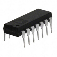
Manufacturer Part Number
AD713JN
Description
IC OPAMP BIFET QUAD PREC 14DIP
Manufacturer
Analog Devices Inc
Datasheet
1.AD713JRZ-16.pdf
(14 pages)
Specifications of AD713JN
Slew Rate
20 V/µs
Rohs Status
RoHS non-compliant
Amplifier Type
J-FET
Number Of Circuits
4
-3db Bandwidth
4MHz
Current - Input Bias
55pA
Voltage - Input Offset
300µV
Current - Supply
10mA
Current - Output / Channel
25mA
Voltage - Supply, Single/dual (±)
9 V ~ 36 V, ±4.5 V ~ 18 V
Operating Temperature
0°C ~ 70°C
Mounting Type
Through Hole
Package / Case
14-DIP (0.300", 7.62mm)
Op Amp Type
General Purpose
No. Of Amplifiers
4
Bandwidth
4MHz
No. Of Pins
14
Operating Temperature Range
0°C To +70°C
Settling Time
1200ns
Operating Temperature Max
70°C
Output Type
-
Gain Bandwidth Product
-
Lead Free Status / RoHS Status
Contains lead / RoHS non-compliant
Available stocks
Company
Part Number
Manufacturer
Quantity
Price

Part Number:
AD713JN
Manufacturer:
ADI/亚德诺
Quantity:
20 000
Company:
Part Number:
AD713JNZ
Manufacturer:
Analog Devices Inc
Quantity:
1 797
Part Number:
AD713JNZ
Manufacturer:
ADI/亚德诺
Quantity:
20 000


Parameter
INPUT OFFSET VOLTAGE
INPUT BIAS CURRENT
INPUT OFFSET CURRENT
MATCHING CHARACTERISTICS
FREQUENCY RESPONSE
INPUT IMPEDANCE
INPUT VOLTAGE RANGE
INPUT VOLTAGE NOISE
INPUT CURRENT NOISE
OPEN-LOOP GAIN
OUTPUT CHARACTERISTICS
POWER SUPPLY
TRANSISTOR COUNT
NOTES
Specifications subject to change without notice.
AD713–SPECIFICATIONS
1
2
3
4
Input Offset Voltage specifications are guaranteed after 5 minutes of operation at T
Bias Current specifications are guaranteed maximum at either input after 5 minutes of operation at T
Defined as voltage between inputs, such that neither exceeds 10 V from ground.
Typically exceeding –14.1 V negative common-mode voltage on either input results in an output phase reversal.
Initial Offset
Offset
vs. Temp
vs. Supply
Long-Term Stability
Input Offset Voltage
Input Offset Voltage Drift
Input Bias Current
Crosstalk
Small Signal Bandwidth
Full Power Response
Slew Rate
Settling Time to 0.01%
Total Harmonic Distortion
Differential
Common Mode
Differential
Common-Mode Voltage
Common Mode
Rejection Ratio
Voltage
Current
Rated Performance
Operating Range
Quiescent Current
3
2
4
1
Conditions
T
T
V
V
V
V
V
T
f = 1 kHz
f = 100 kHz
Unity Gain
V
Unity Gain
f = 1 kHz; R
V
T
V
T
V
T
0.1 Hz to 10 Hz
f = 10 Hz
f = 100 Hz
f = 1 kHz
f = 10 kHz
f = 1 kHz
V
T
R
T
Short Circuit
# of Transistors
CM
CM
CM
CM
CM
O
O
CM
CM
O
L
MIN
MIN
MIN
MIN
MIN
MIN
MIN
MIN
= 20 V p-p
= 3 V rms
= 10 V; R
= 0 V
= 0 V @ T
= 10 V
= 0 V
= 0 V @ T
= 10 V
= 11 V
2 k
to T
to T
to T
to T
to T
to T
to T
to T
MAX
MAX
MAX
MAX
MAX
MAX
MAX
MAX
L
L
MAX
MAX
2 k ;
2 k
(V
S
=
Min
78
76/76/76
3.0
16
–11
78
76/76/76
72
70/70/70
150
100/100/100
+13, –12.5
12/ 12/ 12 +13.8, –13.1
4.5
15 V @ T
A
= 25 C.
A
AD713J/A/S
Typ
0.3
0.5
5
95
95
15
40
55
10
0.5
0.7
8
10
4.0
200
20
1.0
0.0003
3 10
3 10
+14.5, –11.5
88
84
84
80
2
45
22
18
16
0.01
400
+13.9, –13.3
25
10.0
120
= 25 C unless otherwise noted)
20
15
12
12
5.5
5.5
A
= 25 C. For higher temperatures, the current doubles every 10 C.
Max
2/2/2
2.3/2.3/2.3
+13
1.5
150
3.4/9.6/154
200
75
1.7/4.8/77
1.8
100
–130
–95
1.2
13.5
18
Min
84
84
3.4
18
–11
84
82
78
74
200
100
+13, –12.5 +13.9, –13.3
12
4.5
Typ
0.2
0.4
100
100
40
55
10
0.4
0.6
10
4.0
20
0.0003
3 10
3 10
+14.5, –11.5
94
90
90
84
400
+13.8, –13.1
10.0
5
15
6
200
1.0
2
45
22
18
16
0.01
25
120
AD713K/B/T
20
15
12
12
5.5
5.5
Max
0.5
0.7/0.7/1.0 mV
20/20/15
75
1.7/4.8/77
120
35
0.8/2.2/36
0.8
1.0/1.0/1.3 mV
25
35
–130
–95
1.2
+13
12.0
18
Unit
mV
dB
dB
pA
nA
pA
pA
nA
mV
pA
dB
dB
MHz
kHz
V/ s
%
V
V
V
dB
dB
dB
dB
nV/ Hz
nV/ Hz
nV/ Hz
nV/ Hz
pA/ Hz
V/mV
V/mV
V
V
mA
V
V
mA
V/ C
V/Month
V/ C
s
V p-p
pF
pF
Related parts for AD713JN
Image
Part Number
Description
Manufacturer
Datasheet
Request
R

Part Number:
Description:
±1.7g Dual-Axis IMEMS Accelerometer Evaluation Board
Manufacturer:
Analog Devices Inc
Datasheet:

Part Number:
Description:
Inertial Sensor Evaluation System
Manufacturer:
Analog Devices Inc
Datasheet:
Part Number:
Description:
Manufacturer:
Analog Devices Inc
Datasheet:
Part Number:
Description:
Manufacturer:
Analog Devices Inc
Datasheet:
Part Number:
Description:
Manufacturer:
Analog Devices Inc
Datasheet:
Part Number:
Description:
Manufacturer:
Analog Devices Inc
Datasheet:
Part Number:
Description:
Manufacturer:
Analog Devices Inc
Datasheet:
Part Number:
Description:
Manufacturer:
Analog Devices Inc
Datasheet:
Part Number:
Description:
Manufacturer:
Analog Devices Inc
Datasheet:
Part Number:
Description:
Manufacturer:
Analog Devices Inc
Datasheet:
Part Number:
Description:
Manufacturer:
Analog Devices Inc
Datasheet:
Part Number:
Description:
Manufacturer:
Analog Devices Inc
Datasheet:
Part Number:
Description:
Manufacturer:
Analog Devices Inc
Datasheet: