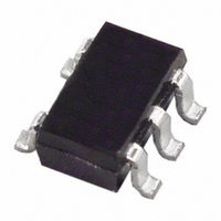
AD8061ART-REEL7 Analog Devices Inc, AD8061ART-REEL7 Datasheet - Page 15

AD8061ART-REEL7
Manufacturer Part Number
AD8061ART-REEL7
Description
IC OPAMP VF R-R LP 50MA SOT23-5
Manufacturer
Analog Devices Inc
Datasheet
1.AD8061ARTZ-REEL7.pdf
(20 pages)
Specifications of AD8061ART-REEL7
Slew Rate
650 V/µs
Rohs Status
RoHS non-compliant
Amplifier Type
Voltage Feedback
Number Of Circuits
1
Output Type
Rail-to-Rail
-3db Bandwidth
320MHz
Current - Input Bias
3.5µA
Voltage - Input Offset
1000µV
Current - Supply
6.8mA
Current - Output / Channel
50mA
Voltage - Supply, Single/dual (±)
2.7 V ~ 8 V, ±1.35 V ~ 4 V
Operating Temperature
-40°C ~ 85°C
Mounting Type
Surface Mount
Package / Case
SOT-23-5, SC-74A, SOT-25
Op Amp Type
Voltage Feedback
No. Of Amplifiers
1
Bandwidth
300MHz
Supply Voltage Range
2.7V To 8V
Amplifier Case Style
SOT-23
No. Of Pins
5
Gain Bandwidth Product
-
Lead Free Status / RoHS Status
Contains lead / RoHS non-compliant
Other names
AD8061ART-REEL7
AD8061ART-REEL7TR
AD8061ART-REEL7TR
Available stocks
Company
Part Number
Manufacturer
Quantity
Price
Company:
Part Number:
AD8061ART-REEL7
Manufacturer:
AD
Quantity:
5 321
Company:
Part Number:
AD8061ART-REEL7
Manufacturer:
AD
Quantity:
129 800
Company:
Part Number:
AD8061ART-REEL7
Manufacturer:
AD
Quantity:
155 170
Part Number:
AD8061ART-REEL7
Manufacturer:
ADI/亚德诺
Quantity:
20 000
Company:
Part Number:
AD8061ART-REEL7/
Manufacturer:
AD
Quantity:
3 000
Company:
Part Number:
AD8061ART-REEL7/HGA
Manufacturer:
MOLEX
Quantity:
2 698
As the saturation point of the output stage is approached, the
output signal shows increasing amounts of compression and
clipping. As in the input headroom case, the higher frequency
signals require a bit more headroom than lower frequency
signals. Figure 16, Figure 17, and Figure 18 illustrate this point,
plotting typical distortion vs. output amplitude and bias for
gains of 2 and 5.
OVERLOAD BEHAVIOR AND RECOVERY
Input
The specified input common-mode voltage of the AD8061/
AD8062/AD8063 is −200 mV below the negative supply to
within 1.8 V of the positive supply. Exceeding the top limit
results in lower bandwidth and increased settling time as seen
in Figure 46 and Figure 47. Pushing the input voltage of a unity-
gain follower beyond 1.6 V within the positive supply leads to
the behavior shown in Figure 48—an increasing amount of
output error and much increased settling time. Recovery time
from input voltages 1.6 V or closer to the positive supply is
approximately 35 ns, which is limited by the settling artifacts
caused by transistors in the input stage coming out of saturation.
The AD8061/AD8062/AD8063 family does not exhibit phase
reversal, even for input voltages beyond the voltage supply rails.
Going more than 0.6 V beyond the power supplies turns on
protection diodes at the input stage, which greatly increases the
current draw of the device.
3.6
3.4
3.2
3.0
2.8
2.6
2.4
2.2
2.0
0
Figure 47. Output Rising Edge for 1 V Step at
Input Headroom Limits, G = 1, V
4
8
12
2V TO 3V STEP
TIME (ns)
16
2.1V TO 3.1V STEP
2.2V TO 3.2V STEP
20
2.3V TO 3.3V STEP
S
= 5 V, 0 V
2.4V TO 3.4V STEP
24
28
32
Rev. G | Page 15 of 20
Output
Output overload recovery is typically within 40 ns after the
amplifier’s input is brought to a nonoverloading value. Figure 49
shows output recovery transients for the amplifier recovering
from a saturated output from the top and bottom supplies to a
point at midsupply.
–0.2
5.0
4.6
4.2
3.8
3.4
3.0
2.6
2.2
1.8
1.4
1.0
0.6
0.2
3.7
3.5
3.3
3.1
2.9
2.7
2.5
2.3
2.1
0
0
INPUT VOLTAGE
Figure 49. Overload Recovery, G = −1, V
Figure 48. Pulse Response for G = 1 Follower,
VOLTAGE STEP
FROM 2.4V TO 3.4V
Input Step Overloading the Input Stage
10
100
EDGES
VOLTAGE STEP
FROM 2.4V TO 3.6V
20
200
AD8061/AD8062/AD8063
30
VOLTAGE STEP
FROM 2.4V TO 3.8V,
4V AND 5V
TIME (ns)
TIME (ns)
300
40
V
–
IN
400
2.5V
50
OUTPUT VOLTAGE
5V TO 2.5V
R
OUTPUT VOLTAGE
0V TO 2.5V
S
500
= 5 V
60
R
5V
600
70
V
O
–


