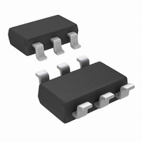
LMV791MK/NOPB National Semiconductor, LMV791MK/NOPB Datasheet - Page 4

LMV791MK/NOPB
Manufacturer Part Number
LMV791MK/NOPB
Description
IC OP AMP CMOS 1.8V TSOT23-6
Manufacturer
National Semiconductor
Series
PowerWise®r
Datasheet
1.LMV792MMNOPB.pdf
(22 pages)
Specifications of LMV791MK/NOPB
Amplifier Type
General Purpose
Number Of Circuits
1
Output Type
Rail-to-Rail
Slew Rate
11.5 V/µs
Gain Bandwidth Product
17MHz
Current - Input Bias
0.1pA
Voltage - Input Offset
100µV
Current - Supply
1.15mA
Current - Output / Channel
60mA
Voltage - Supply, Single/dual (±)
1.8 V ~ 5.5 V
Operating Temperature
-40°C ~ 125°C
Mounting Type
Surface Mount
Package / Case
TSOT-23-6, TSOT-6
Lead Free Status / RoHS Status
Lead free / RoHS Compliant
-3db Bandwidth
-
Other names
LMV791MK
LMV791MKNOPB
LMV791MKNOPBTR
LMV791MKNOPBTR
LMV791MKTR
LMV791MKNOPB
LMV791MKNOPBTR
LMV791MKNOPBTR
LMV791MKTR
www.national.com
A
V
I
I
SR
GBW
e
i
t
t
V
I
THD+N Total Harmonic Distortion + Noise
n
OUT
S
on
off
EN
n
VOL
OUT
EN
Note 1: Absolute Maximum Ratings indicate limits beyond which damage to the device may occur. Operating Ratings indicate conditions for which the device is
intended to be functional, but specific performance is not guaranteed. For guaranteed specifications and the test conditions, see the Electrical Characteristics
Tables.
Note 2: Human Body Model is 1.5 kΩ in series with 100 pF. Machine Model is 0Ω in series with 200 pF
Note 3: The maximum power dissipation is a function of T
P
Note 4: Typical values represent the parametric norm at the time of characterization.
Note 5: Limits are 100% production tested at 25°C. Limits over the operating temperature range are guaranteed through correlations using the statistical quality
control (SQC) method.
Note 6: Offset voltage average drift is determined by dividing the change in V
Note 7: Positive current corresponds to current flowing into the device.
Note 8: This parameter is guaranteed by design and/or characterization and is not tested in production.
Note 9: The short circuit test is a momentary test, the short circuit duration is 1.5 ms.
D
= (T
J(MAX)
Open Loop Voltage Gain
Output Voltage Swing High
Output Voltage Swing Low
Output Current
Supply Current per Amplifier
Slew Rate
Gain Bandwidth
Input Referred Voltage Noise Density
Input Referred Current Noise Density
Turn-on Time
Turn-off Time
Enable Pin Voltage Range
Enable Pin Input Current
- T
A
)/θ
JA
. All numbers apply for packages soldered directly onto a PC Board.
J(MAX)
V
R
V
R
R
R
R
R
Sourcing to V
V
Sinking to V
V
Enable Mode
V
Shutdown Mode (V
A
A
f = 1 kHz
f = 1 kHz
Enable Mode
Shutdown Mode
Enable Mode V
(Note 7)
Shutdown Mode V
(Note 7)
f = 1 kHz, A
OUT
OUT
IN
IN
EN
V
V
LOAD
LOAD
LOAD
LOAD
LOAD
LOAD
= +1, Rising (10% to 90%)
= +1, Falling (90% to 10%)
= 200 mV (Note 9)
= –200 mV (Note 9)
, θ
≥
= 0.3V to 4.7V,
= 0.3V to 4.7V,
JA
4.6V
= 2 kΩ to V
= 10 kΩ to V
= 2 kΩ to V
= 10 kΩ to V
= 2 kΩ to V
= 10 kΩ to V
. The maximum allowable power dissipation at any ambient temperature is
V
+
= 1, R
−
OS
EN
4
by temperature change.
+
+
+
= 5.0V
EN
/2
/2
/2 LMV791
+
+
+
EN
LOAD
/2
/2
/2
= 0V
≤
LMV791
LMV792
LMV792
LMV791
LMV792
per channel
0.4V)
= 600Ω
6.0
7.5
4.6
85
80
82
78
88
84
45
37
10
6
4.5 to 5
0 to 0.5
0.005
1.15
1.30
0.14
11.5
0.01
0.01
110
110
800
9.5
5.8
5.6
97
89
35
25
42
45
20
60
21
17
1.40
1.75
1.70
2.05
0.4
0.2
75
82
65
71
75
78
80
83
65
67
10
1
5
either rail
mV from
nV/
pA/
MHz
V/μs
mA
mA
dB
μA
μA
ns
ns
%
V


