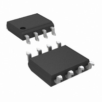
LMH6628MA/NOPB National Semiconductor, LMH6628MA/NOPB Datasheet - Page 9

LMH6628MA/NOPB
Manufacturer Part Number
LMH6628MA/NOPB
Description
IC OP AMP DUAL 2CH LN 8-SOIC
Manufacturer
National Semiconductor
Series
PowerWise®r
Datasheet
1.LMH6628MANOPB.pdf
(11 pages)
Specifications of LMH6628MA/NOPB
Amplifier Type
Voltage Feedback
Number Of Circuits
2
Slew Rate
550 V/µs
Gain Bandwidth Product
200MHz
-3db Bandwidth
300MHz
Current - Input Bias
700nA
Voltage - Input Offset
500µV
Current - Supply
9mA
Current - Output / Channel
85mA
Voltage - Supply, Single/dual (±)
5 V ~ 12 V, ±2.5 V ~ 6 V
Operating Temperature
-40°C ~ 85°C
Mounting Type
Surface Mount
Package / Case
8-SOIC (3.9mm Width)
Lead Free Status / RoHS Status
Lead free / RoHS Compliant
Output Type
-
Other names
*LMH6628MA
*LMH6628MA/NOPB
LMH6628MA
*LMH6628MA/NOPB
LMH6628MA
Application Section
The circuit gain is +1 and the delay is determined by the
following equations.
where T
The LMH6628 provides a typical delay of 2.8ns at its −3dB
point.
FULL DUPLEX DIGITAL OR ANALOG TRANSMISSION
Simultaneous transmission and reception of analog or digital
signals over a single coaxial cable or twisted-pair line can
reduce cabling requirements. The LMH6628’s wide band-
width and high common-mode rejection in a differential am-
plifier configuration allows full duplex transmission of video,
telephone, control and audio signals.
In the circuit shown in Figure 3, one of the LMH6628’s amps
is used as a "driver" and the other as a difference "receiver"
amplifier. The output impedance of the "driver" is essentially
zero. The two R’s are chosen to match the characteristic
impedance of the transmission line. The "driver" op amp gain
can be selected for unity or greater.
Receiver amplifier A
differential amplifier for the signals transmitted by driver A
(B
signals from driver A
B
The output of the receiver amplifier will be:
Care must be given to layout and component placement to
maintain a high frequency common-mode rejection. The plot
of Figure 4 shows the simultaneous reception of signals
transmitted at 1MHz and 10MHz.
1
2
). If R
(A
1
).
d
F
is the delay of the op amp at A
equals R
2
G
1
(B
, receiver A
T
(B
d
2
FIGURE 3.
1
) is connected across R and forms
) and pass the signals from driver
=
360
1
d
df
2
φ
(Continued)
(B
;
1
) will then reject the
V
= +1.
20038503
(1)
(2)
(3)
2
9
POSITIVE PEAK DETECTOR
The LMH6628’s dual amplifiers can be used to implement a
unity-gain peak detector circuit as shown in Figure 5.
The acquisition speed of this circuit is limited by the dynamic
resistance of the diode when charging C
circuit’s performance is shown in Figure 6 with a 1MHz
sinusoidal input.
FIGURE 4.
FIGURE 5.
hold
20038531
. A plot of the
www.national.com
20038505


