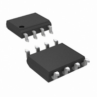
LMH6628MA/NOPB National Semiconductor, LMH6628MA/NOPB Datasheet - Page 8

LMH6628MA/NOPB
Manufacturer Part Number
LMH6628MA/NOPB
Description
IC OP AMP DUAL 2CH LN 8-SOIC
Manufacturer
National Semiconductor
Series
PowerWise®r
Datasheet
1.LMH6628MANOPB.pdf
(11 pages)
Specifications of LMH6628MA/NOPB
Amplifier Type
Voltage Feedback
Number Of Circuits
2
Slew Rate
550 V/µs
Gain Bandwidth Product
200MHz
-3db Bandwidth
300MHz
Current - Input Bias
700nA
Voltage - Input Offset
500µV
Current - Supply
9mA
Current - Output / Channel
85mA
Voltage - Supply, Single/dual (±)
5 V ~ 12 V, ±2.5 V ~ 6 V
Operating Temperature
-40°C ~ 85°C
Mounting Type
Surface Mount
Package / Case
8-SOIC (3.9mm Width)
Lead Free Status / RoHS Status
Lead free / RoHS Compliant
Output Type
-
Other names
*LMH6628MA
*LMH6628MA/NOPB
LMH6628MA
*LMH6628MA/NOPB
LMH6628MA
www.national.com
Typical Performance Characteristics
specified) (Continued)
Application Section
LOW NOISE DESIGN
Ultimate low noise performance from circuit designs using
the LMH6628 requires the proper selection of external resis-
tors. By selecting appropriate low valued resistors for R
R
noise that is approximately the equivalent voltage input
noise of 2nV/
DC BIAS CURRENTS AND OFFSET VOLTAGES
Cancellation of the output offset voltage due to input bias
currents is possible with the LMH6628. This is done by
making the resistance seen from the inverting and non-
inverting inputs equal. Once done, the residual output offset
voltage will be the input offset voltage (V
desired gain (A
several solutions to further reduce the output offset.
OUTPUT AND SUPPLY CONSIDERATIONS
With
output swing of
output swing is possible with slightly higher supply voltages.
For loads of less than 50Ω, the output swing will be limited by
the LMH6628’s output current capability, typically 85mA.
Output settling time when driving capacitive loads can be
improved by the use of a series output resistor. See the plot
labeled "R
LAYOUT
Proper power supply bypassing is critical to insure good high
frequency performance and low noise. De-coupling capaci-
tors of 0.1µF should be placed as close as possible to the
power supply pins. The use of surface mounted capacitors is
recommended due to their low series inductance.
A good high frequency layout will keep power supply and
ground traces away from the inverting input and output pins.
Parasitic capacitance from these nodes to ground causes
frequency response peaking and possible circuit oscillation.
G
, amplifier circuits using the LMH6628 can achieve output
±
5V supplies, the LMH6628 is capable of a typical
S
vs. C
±
V
). National Application Note OA-7 offers
3.8V under a no-load condition. Additional
L
" in the Typical Performance section.
multiplied by the desired gain (A
OS
) multiplied by the
Settling Time vs. Accuracy
V
).
F
and
(T
8
A
= +25˚, A
See OA-15 for more information. National suggests the
730036 (SOIC) dual op amp evaluation board as a guide for
high frequency layout and as an aid in device evaluation.
ANALOG DELAY CIRCUIT (ALL-PASS NETWORK)
The circuit in Figure 1 implements an all-pass network using
the LMH6628. A wide bandwidth buffer (LM7121) drives the
circuit and provides a high input impedance for the source.
As shown in Figure 2, the circuit provides a 13.1ns delay
(with R = 40.2Ω, C = 47pF). R
and low value for parasitic insensitive operation.
FIGURE 2. Delay Circuit Response to 0.5V Pulse
V
= +2, V
20038548
CC
=
±
FIGURE 1.
5V, R
f
F
=100Ω, R
and R
G
should be of equal
L
= 100Ω, unless
20038502
20038501


