OP495GPZ Analog Devices Inc, OP495GPZ Datasheet - Page 2
OP495GPZ
Manufacturer Part Number
OP495GPZ
Description
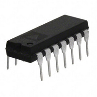
IC OPAMP GP R-R 85KHZ QUAD 14DIP
Manufacturer
Analog Devices Inc
Datasheet
1.OP295GPZ.pdf
(16 pages)
Specifications of OP495GPZ
Slew Rate
0.03 V/µs
Amplifier Type
General Purpose
Number Of Circuits
4
Output Type
Rail-to-Rail
Gain Bandwidth Product
85kHz
Current - Input Bias
7nA
Voltage - Input Offset
300µV
Current - Supply
175µA
Current - Output / Channel
25mA
Voltage - Supply, Single/dual (±)
3 V ~ 36 V, ±1.5 V ~ 18 V
Operating Temperature
-40°C ~ 125°C
Mounting Type
Through Hole
Package / Case
14-DIP (0.300", 7.62mm)
Op Amp Type
Low Offset Voltage
No. Of Amplifiers
1
Bandwidth
85kHz
Supply Voltage Range
± 1.5V To ± 15V
Amplifier Case Style
DIP
No. Of Pins
14
Lead Free Status / RoHS Status
Lead free / RoHS Compliant
-3db Bandwidth
-
Lead Free Status / RoHS Status
Lead free / RoHS Compliant, Lead free / RoHS Compliant


OP295/OP495
TABLE OF CONTENTS
Features .............................................................................................. 1
Applications ....................................................................................... 1
General Description ......................................................................... 1
Pin Configurations ........................................................................... 1
Revision History ............................................................................... 2
Specifications ..................................................................................... 3
Absolute Maximum Ratings ............................................................ 5
Typical Performance Characteristics ............................................. 6
Applications ....................................................................................... 9
REVISION HISTORY
8/09—Rev. F to Rev. G
Added Figure 18 ................................................................................ 8
Updated Outline Dimensions ....................................................... 17
3/08—Rev. E to Rev. F
Changes to Offset Voltage Unit in Table 1 .................................... 3
Updated Outline Dimensions ....................................................... 14
Changes to Ordering Guide .......................................................... 16
5/06—Rev. D to Rev. E
Updated Format .................................................................. Universal
Changes to Features .......................................................................... 1
Changes to Pin Connections ........................................................... 1
Updated Outline Dimensions ....................................................... 14
Changes to Ordering Guide .......................................................... 15
2/04—Rev. C to Rev. D
Changes to General Description .................................................... 1
Changes to Specifications ................................................................ 2
Changes to Absolute Maximum Ratings ....................................... 4
Changes to Ordering Guide ............................................................ 4
Updated Outline Dimensions ....................................................... 12
Electrical Characteristics ............................................................. 3
Thermal Resistance ...................................................................... 5
ESD Caution .................................................................................. 5
Rail-to-Rail Application Information ........................................ 9
Low Drop-Out Reference ............................................................ 9
Low Noise, Single-Supply Preamplifier ..................................... 9
Driving Heavy Loads ................................................................. 10
Rev. G | Page 2 of 16
Outline Dimensions ....................................................................... 14
3/02—Rev. B to Rev. C
Figure changes to Pin Connections ................................................ 1
Deleted OP295GBC and OP495GBC from Ordering Guide ...... 3
Deleted Wafer Test Limits Table ...................................................... 3
Changes to Absolute Maximum Ratings ........................................ 4
Deleted Dice Characteristics ............................................................ 4
Direct Access Arrangement ...................................................... 10
Single-Supply Instrumentation Amplifier .............................. 10
Single-Supply RTD Thermometer Amplifier ......................... 11
Cold Junction Compensated, Battery-Powered
Thermocouple Amplifier .......................................................... 11
5 V Only, 12-Bit DAC That Swings 0 V to 4.095 V .................... 11
4 mA to 20 mA Current-Loop Transmitter ............................ 12
3 V Low Dropout Linear Voltage Regulator ............................. 12
Low Dropout, 500 mA Voltage Regulator with Foldback
Current Limiting ........................................................................ 12
Square Wave Oscillator .............................................................. 13
Single-Supply Differential Speaker Driver .............................. 13
High Accuracy, Single-Supply, Low Power Comparator ...... 13
Ordering Guide .......................................................................... 16
Related parts for OP495GPZ
Image
Part Number
Description
Manufacturer
Datasheet
Request
R

Part Number:
Description:
±1.7g Dual-Axis IMEMS Accelerometer Evaluation Board
Manufacturer:
Analog Devices Inc
Datasheet:

Part Number:
Description:
Inertial Sensor Evaluation System
Manufacturer:
Analog Devices Inc
Datasheet:
Part Number:
Description:
Manufacturer:
Analog Devices Inc
Datasheet:
Part Number:
Description:
Manufacturer:
Analog Devices Inc
Datasheet:
Part Number:
Description:
Manufacturer:
Analog Devices Inc
Datasheet:
Part Number:
Description:
Manufacturer:
Analog Devices Inc
Datasheet:
Part Number:
Description:
Manufacturer:
Analog Devices Inc
Datasheet:
Part Number:
Description:
Manufacturer:
Analog Devices Inc
Datasheet:
Part Number:
Description:
Manufacturer:
Analog Devices Inc
Datasheet:
Part Number:
Description:
Manufacturer:
Analog Devices Inc
Datasheet:
Part Number:
Description:
Manufacturer:
Analog Devices Inc
Datasheet:
Part Number:
Description:
Manufacturer:
Analog Devices Inc
Datasheet:
Part Number:
Description:
Manufacturer:
Analog Devices Inc
Datasheet: