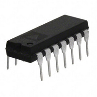
OP495GPZ Analog Devices Inc, OP495GPZ Datasheet

OP495GPZ
Specifications of OP495GPZ
Related parts for OP495GPZ
OP495GPZ Summary of contents
Page 1
FEATURES Rail-to-rail output swing Single-supply operation Low offset voltage: 300 μV Gain bandwidth product: 75 kHz High open-loop gain: 1000 V/mV Unity-gain stable Low supply current/per amplifier: 150 μA maximum APPLICATIONS Battery-operated instrumentation Servo amplifiers ...
Page 2
OP295/OP495 TABLE OF CONTENTS Features .............................................................................................. 1 Applications ....................................................................................... 1 General Description ......................................................................... 1 Pin Configurations ........................................................................... 1 Revision History ............................................................................... 2 Specifications ..................................................................................... 3 Electrical Characteristics ............................................................. 3 Absolute Maximum Ratings ............................................................ 5 Thermal Resistance ...................................................................... 5 ESD Caution ...
Page 3
SPECIFICATIONS ELECTRICAL CHARACTERISTICS 25°C, unless otherwise noted Table 1. Parameter Symbol INPUT CHARACTERISTICS Offset Voltage V Input Bias Current I Input Offset Current I Input Voltage Range ...
Page 4
OP295/OP495 Parameter Symbol OUTPUT CHARACTERISTICS Output Voltage Swing High V Output Voltage Swing Low V POWER SUPPLY Power Supply Rejection Ratio PSRR Supply Current per Amplifier I DYNAMIC PERFORMANCE Slew Rate SR Gain Bandwidth Product GBP Phase Margin θ NOISE ...
Page 5
ABSOLUTE MAXIMUM RATINGS Table 4. 1 Parameter Supply Voltage Input Voltage 2 Differential Input Voltage Output Short-Circuit Duration Storage Temperature Range P, S Packages Operating Temperature Range OP295G, OP495G Junction Temperature Range P, S Packages Lead Temperature (Soldering, 60 sec) ...
Page 6
OP295/OP495 TYPICAL PERFORMANCE CHARACTERISTICS 140 120 100 –50 – TEMPERATURE (°C) Figure 5. Supply Current Per Amplifier vs. Temperature 15.2 V 15.0 14.8 14.6 14.4 14.2 –14.4 –14.6 –14.8 –15.0 –15.2 –50 –25 0 ...
Page 7
BASED ON 1200 OP AMPS 450 400 350 300 250 200 150 100 50 0 –100 – 100 150 200 INPUT OFFSET VOLTAGE (µV) Figure 11. OP495 Input Offset (V ) Distribution OS 500 BASED ON 1200 ...
Page 8
OP295/OP495 25° 100mV SOURCE 10mV SINK 1mV 100µV 1µA 10µA 100µA 1mA LOAD CURRENT Figure 17. Output Voltage to Supply Rail vs. Load Current 120 100 OP295 ...
Page 9
APPLICATIONS RAIL-TO-RAIL APPLICATION INFORMATION The OP295/OP495 have a wide common-mode input range extending from ground to within about 800 mV of the positive supply. There is a tendency to use the OP295/OP495 in buffer applications where the input voltage could ...
Page 10
OP295/OP495 Finally, the potentiometer, R8, is needed to adjust the offset voltage to null it to zero. Similar performance can be obtained using an OP90 as the output amplifier with a savings of about 185 μA of supply current. However, ...
Page 11
V IN OP295/ 6 OP495 – – 100kΩ 20kΩ 20kΩ V REF 200kΩ REF R G Figure ...
Page 12
OP295/OP495 17.8kΩ DAC8043 1.23V I REF OUT 2 GND CLK SRI LD AD589 41.2kΩ DIGITAL CONTROL R3 5kΩ TOTAL POWER DISSIPATION = ...
Page 13
Amplifier A1 provides error amplification for the normal voltage regulation loop. As long as the output current is less than 1 A, the output of Amplifier A2 swings to ground, reverse- biasing the diode and effectively taking itself out of ...
Page 14
OP295/OP495 OUTLINE DIMENSIONS 0.210 (5.33) MAX 0.150 (3.81) 0.130 (3.30) 0.115 (2.92) 0.022 (0.56) 0.018 (0.46) 0.014 (0.36) CONTROLLING DIMENSIONS ARE IN INCHES; MILLIMETER DIMENSIONS (IN PARENTHESES) ARE ROUNDED-OFF INCH EQUIVALENTS FOR REFERENCE ONLY AND ARE NOT APPROPRIATE FOR USE ...
Page 15
BSC 0.210 (5.33) MAX 0.015 0.150 (3.81) (0.38) MIN 0.130 (3.30) 0.110 (2.79) SEATING PLANE 0.022 (0.56) 0.005 (0.13) 0.018 (0.46) MIN ...
Page 16
... OP295GSZ −40°C to +125°C 1 OP295GSZ-REEL −40°C to +125°C 1 OP295GSZ-REEL7 −40°C to +125°C OP495GP −40°C to +125°C 1 OP495GPZ −40°C to +125°C OP495GS −40°C to +125°C OP495GS-REEL −40°C to +125°C 1 OP495GSZ −40°C to +125°C OP495GSZ-REEL 1 − ...


