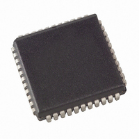
AT90S8515-8JI Atmel, AT90S8515-8JI Datasheet - Page 47

AT90S8515-8JI
Manufacturer Part Number
AT90S8515-8JI
Description
IC MCU 8K FLSH 8MHZ IT 44PLCC
Manufacturer
Atmel
Series
AVR® 90Sr
Datasheets
1.AT90S8515-4AC.pdf
(112 pages)
2.AT90S8515-4AC.pdf
(4 pages)
3.AT90S8515-4AC.pdf
(4 pages)
Specifications of AT90S8515-8JI
Core Processor
AVR
Core Size
8-Bit
Speed
8MHz
Connectivity
SPI, UART/USART
Peripherals
Brown-out Detect/Reset, POR, PWM, WDT
Number Of I /o
32
Program Memory Size
8KB (4K x 16)
Program Memory Type
FLASH
Eeprom Size
512 x 8
Ram Size
512 x 8
Voltage - Supply (vcc/vdd)
4 V ~ 6 V
Oscillator Type
Internal
Operating Temperature
-40°C ~ 85°C
Package / Case
44-PLCC
Lead Free Status / RoHS Status
Contains lead / RoHS non-compliant
Data Converters
-
Available stocks
Company
Part Number
Manufacturer
Quantity
Price
Company:
Part Number:
AT90S8515-8JI
Manufacturer:
ATM
Quantity:
4 500
Company:
Part Number:
AT90S8515-8JI
Manufacturer:
ATM
Quantity:
4 500
Part Number:
AT90S8515-8JI
Manufacturer:
ATMEL/爱特梅尔
Quantity:
20 000
Serial Peripheral
Interface – SPI
0841G–09/01
The Serial Peripheral Interface (SPI) allows high-speed synchronous data transfer
between the AT90S8515 and peripheral devices or between several AVR devices. The
AT90S8515 SPI features include the following:
•
•
•
•
•
•
•
Figure 34. SPI Block Diagram
The interconnection between master and slave CPUs with SPI is shown in Figure 35.
The PB7(SCK) pin is the clock output in the Master Mode and is the clock input in the
Slave Mode. Writing to the SPI Data Register of the master CPU starts the SPI clock
generator and the data written shifts out of the PB5(MOSI) pin and into the PB5(MOSI)
pin of the slave CPU. After shifting one byte, the SPI clock generator stops, setting the
end-of-transmission flag (SPIF). If the SPI interrupt enable bit (SPIE) in the SPCR regis-
ter is set, an interrupt is requested. The Slave Select input, PB4(SS), is set low to select
an individual slave SPI device. The two shift registers in the master and the slave can be
considered as one distributed 16-bit circular shift register. This is shown in Figure 35.
When data is shifted from the master to the slave, data is also shifted in the opposite
direction, simultaneously. This means that during one shift cycle, data in the master and
the slave are interchanged.
Full-duplex, 3-wire Synchronous Data Transfer
Master or Slave Operation
LSB First or MSB First Data Transfer
Four Programmable Bit Rates
End-of-Transmission Interrupt Flag
Write Collision Flag Protection
Wake-up from Idle Mode (Slave Mode Only)
AT90S8515
47


