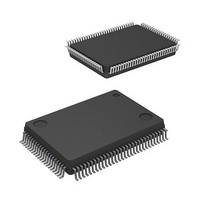
R5F363AENFA#U0 Renesas Electronics America, R5F363AENFA#U0 Datasheet - Page 47

R5F363AENFA#U0
Manufacturer Part Number
R5F363AENFA#U0
Description
MCU 4KB FLASH 256/16K 100-QFP
Manufacturer
Renesas Electronics America
Series
M16C/60/63r
Specifications of R5F363AENFA#U0
Core Processor
M16C/60
Core Size
16/32-Bit
Speed
20MHz
Connectivity
EBI/EMI, I²C, SIO, UART/USART
Peripherals
DMA, LVD, POR, PWM, WDT
Number Of I /o
85
Program Memory Size
256KB (256K x 8)
Program Memory Type
FLASH
Ram Size
20K x 8
Voltage - Supply (vcc/vdd)
1.8 V ~ 5.5 V
Data Converters
A/D 26x10b; D/A 2x8b
Oscillator Type
Internal
Operating Temperature
-20°C ~ 85°C
Package / Case
100-QFP
Lead Free Status / RoHS Status
Lead free / RoHS Compliant
Eeprom Size
-
Available stocks
Company
Part Number
Manufacturer
Quantity
Price
M16C/63 Group
REJ03B0271-0100 Rev.1.00 Sep 15, 2009
Page 45 of 113
4.2
4.2.1
Table 4.17
Watchdog Timer Refresh Register
Watchdog Timer Start Register
Timer A0 Register
Timer A1 Register
Timer A2 Register
Timer A3 Register
Timer A4 Register
Timer A1-1 Register
Timer A2-1 Register
Timer A4-1 Register
Three-Phase Output Buffer Register 0
Three-Phase Output Buffer Register 1
Dead Time Timer
Timer B2 Interrupt Generation Frequency Set Counter
UART0 Bit Rate Register
UART1 Bit Rate Register
UART2 Bit Rate Register
UART5 Bit Rate Register
UART6 Bit Rate Register
UART7 Bit Rate Register
UART0 Transmit Buffer Register
UART1 Transmit Buffer Register
UART2 Transmit Buffer Register
UART5 Transmit Buffer Register
UART6 Transmit Buffer Register
UART7 Transmit Buffer Register
SI/O3 Bit Rate Register
SI/O4 Bit Rate Register
I2C0 Control Register 1
I2C0 Status Register 0
Table 4.17 lists Registers with Write-Only Bits and registers whose function differs between reading and
writing. Set these registers with immediate values. When establishing the next value by altering the
existing value, write the existing value to the RAM as well as to the register. Transfer the next value to
the register after making changes in the RAM.
Notes on SFRs
Register Settings
Registers with Write-Only Bits
Register
U0BRG
U1BRG
U2BRG
U5BRG
U6BRG
U7BRG
Symbol
S3BRG
S4BRG
WDTR
WDTS
ICTB2
U0TB
U2TB
U5TB
U6TB
U7TB
S3D0
U1TB
TA21
TA41
TA11
IDB0
IDB1
DTT
TA0
TA1
TA2
TA3
TA4
S10
4. Special Function Registers (SFRs)
02ABh to 02AAh
032Dh to 032Ch
032Bh to 032Ah
024Bh to 024Ah
025Bh to 025Ah
026Bh to 026Ah
028Bh to 028Ah
029Bh to 029Ah
032Fh to 032Eh
0327h to 0326h
0329h to 0328h
0303h to 0302h
0305h to 0304h
0307h to 0306h
Address
037Dh
030Ah
030Bh
030Ch
030Dh
037Eh
0249h
0259h
0269h
02A9h
02B6h
02B8h
0289h
0299h
0273h
0277h


