R5F363AENFA#U0 Renesas Electronics America, R5F363AENFA#U0 Datasheet
R5F363AENFA#U0
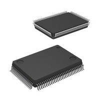
Specifications of R5F363AENFA#U0
Available stocks


Related parts for R5F363AENFA#U0


R5F363AENFA#U0 Summary of contents
Page 1
To our customers, Old Company Name in Catalogs and Other Documents st On April 1 , 2010, NEC Electronics Corporation merged with Renesas Technology Corporation, and Renesas Electronics Corporation took over all the business of both companies. Therefore, although the ...
Page 2
All information included in this document is current as of the date this document is issued. Such information, however, is subject to change without any prior notice. Before purchasing or using any Renesas Electronics products listed herein, please confirm ...
Page 3
M16C/63 Group RENESAS MCU 1. Overview 1.1 Features The M16C/63 Group microcomputer (MCU) incorporates the M16C/60 Series CPU core and flash memory, employing sophisticated instructions for a high level of efficiency. This MCU has address space (expandable ...
Page 4
M16C/63 Group 1.2 Specifications The M16C/63 Group includes 100-pin and 80-pin packages. Table 1.1 to Table 1.4 list specifications. Table 1.1 Specifications for the 100-Pin Package (1/2) Item Function CPU Central processing unit Memory ROM, RAM, data flash Voltage Voltage ...
Page 5
M16C/63 Group Table 1.2 Specifications for the 100-Pin Package (2/2) Item Function Timer A Timer B Three-phase motor control timer functions Timers Real-time clock PWM function Remote control signal receiver UART0 to UART2, UART5 to Serial UART7 Interface SI/O3, SI/O4 ...
Page 6
M16C/63 Group Table 1.3 Specifications for the 80-Pin Package (1/2) Item Function CPU Central processing unit Memory ROM, RAM, data flash Voltage Voltage detector Detection Clock Clock generator External Bus Bus memory expansion Expansion I/O Ports Programmable I/O ports Interrupts ...
Page 7
M16C/63 Group Table 1.4 Specifications for the 80-Pin Package (2/2) Item Function Timer A Timer B Three-phase motor control Timers timer functions Real-time clock PWM function Remote control signal receiver UART0 to UART2, UART5 Serial Interface SI/O3, SI/O4 2 Multi-master ...
Page 8
M16C/63 Group 1.3 Product List Table 1.5 lists product information. Figure 1.1 shows the Part No., with Memory Size and Package, and Figure 1.2 and Figure 1.3 shows the Marking Diagram (Top View). Table 1.5 Product List Part No. Program ...
Page 9
M16C/63 Group Part No Figure 1.1 Part No., with Memory Size and Package PRQP0100JD-B (100P6F-A), PLQP0100KB-A (100P6Q-A), PLQP0080KB-A (80P6Q- ...
Page 10
M16C/63 Group 1.4 Block Diagram Figure 1.4 and Figure 1.5 show block diagrams Port P0 Port P1 Internal peripheral functions Timer (16-bit) Outputs (timer A): 5 Inputs (timer B): 6 Three-phase motor control circuit Real-time clock PWM function ...
Page 11
M16C/63 Group 8 Port P0 Internal peripheral functions Timer (16-bit) Outputs (timer A): 5 Inputs (timer B): 6 Real-time clock PWM function (8-bit x 2) Remote control signal receiver (2 circuits) Watchdog timer (15-bit) A/D converter (10-bit resolution x 26 ...
Page 12
M16C/63 Group 1.5 Pin Assignments Figure 1.6 to Figure 1.9 show pin assignments. Table 1.6 to Table 1.9 list pin names. P0_7/AN0_7/ P0_6/AN0_6/D6 83 P0_5/AN0_5/D5 84 P0_4/AN0_4/D4 85 P0_3/AN0_3/D3 P0_2/AN0_2/ P0_1/AN0_1/D1 88 P0_0/AN0_0/D0 89 P10_7/AN7/KI3 90 ...
Page 13
M16C/63 Group 76 P1_2/RXD6/SCL6/D10 77 P1_1/CLK6/D9 78 P1_0/CTS6/RTS6/D8 79 P0_7/AN0_7/D7 80 P0_6/AN0_6/D6 81 P0_5/AN0_5/D5 82 P0_4/AN0_4/D4 83 P0_3/AN0_3/D3 84 P0_2/AN0_2/D2 85 P0_1/AN0_1/D1 P0_0/AN0_0/ P10_7/AN7/KI3 88 P10_6/AN6/KI2 89 P10_5/AN5/KI1 90 P10_4/AN4/KI0 91 P10_3/AN3/KI7 92 P10_2/AN2/KI6 93 P10_1/AN1/KI5 94 AVSS ...
Page 14
M16C/63 Group P4_2 P4_3 J P4_1 P4_0 H P3_6 P3_7 G P3_2 P3_3 F P3_0 VCC2 E P2_6 P2_7 D P2_2 P2_1 C P2_0 P1_7 B P1_4 P1_5 A P1_3 P1_2 10 9 VCC2 ports Notes: 1. ...
Page 15
M16C/63 Group Table 1.6 Pin Names for the 100-Pin Package (1/2) Pin No. Control Pin Port P9_6 2 100 A2 P9_5 P9_4 P9_3 P9_2 6 ...
Page 16
M16C/63 Group Table 1.7 Pin Names for the 100-Pin Package (2/2) Pin No. Control Port Pin P4_3 52 50 K10 P4_2 53 51 J10 P4_1 P4_0 P3_7 56 ...
Page 17
M16C/63 Group 61 P0_6/AN0_6 P0_5/AN0_5 62 P0_4/AN0_4 63 P0_3/AN0_3 64 P0_2/AN0_2 65 P0_1/AN0_1 66 P0_0/AN0_0 67 P10_7/AN7/KI3 68 P10_6/AN6/KI2 69 P10_5/AN5/KI1 70 P10_4/AN4/KI0 71 P10_3/AN3/KI7 72 P10_2/AN2/KI6 73 P10_1/AN1/KI5 74 AVSS 75 P10_0/AN0/KI4 76 VREF 77 AVCC 78 P9_7/ADTRG/SIN4 79 ...
Page 18
M16C/63 Group Table 1.8 Pin Names for the 80-Pin Package (1/2) Pin No. Control Pin Port 1 P9_5 2 P9_4 3 P9_3 4 P9_2 5 P9_0 6 CNVSS 7 XCIN P8_7 8 XCOUT P8_6 RESET 9 10 XOUT 11 VSS ...
Page 19
M16C/63 Group Table 1.9 Pin Names for the 80-Pin Package (2/2) Pin No. Control Pin Port 41 P4_2 42 P4_1 43 P4_0 44 P3_7 45 P3_6 46 P3_5 47 P3_4 48 P3_3 49 P3_2 50 P3_1 51 P3_0 52 P2_7 ...
Page 20
M16C/63 Group 1.6 Pin Functions Table 1.10 Pin Functions for the 100-Pin Package (1/3) Signal Name Pin Name Power supply VCC1, input VCC2, VSS Analog power AVCC, AVSS supply input RESET Reset input CNVSS CNVSS External data bus BYTE width ...
Page 21
M16C/63 Group Table 1.11 Pin Functions for the 100-Pin Package (2/3) Signal Name Pin Name Main clock input XIN Main clock output XOUT Sub clock input XCIN Sub clock output XCOUT BCLK output BCLK Clock output CLKOUT INT0 to INT2 ...
Page 22
M16C/63 Group Table 1.12 Pin Functions for the 100-Pin Package (3/3) Signal Name Pin Name SDA0 to SDA2, UART0 to SDA5 UART2, SDA6, SDA7 UART5 to SCL0 to SCL2, UART7 SCL5 mode SCL6, SCL7 CLK3, CLK4 Serial ...
Page 23
M16C/63 Group Table 1.13 Pin Functions for the 80-Pin Package (1/2) Signal Name Pin Name Power supply VCC1, input VSS Analog power AVCC, supply input AVSS RESET Reset input CNVSS CNVSS Main clock input XIN Main clock output XOUT Sub ...
Page 24
M16C/63 Group Table 1.14 Pin Functions for the 80-Pin Package (2/2) Signal Name Pin Name CTS0, CTS1, CTS5 RTS0, RTS1, RTS5 CLK0, CLK1, Serial interface CLK5 UART0 to UART2, RXD0 to RXD2, UART5 RXD5 TXD0 to TXD2, TXD5 CLKS1 SDA0 ...
Page 25
M16C/63 Group 2. Central Processing Unit (CPU) Figure 2.1 shows the CPU registers. Seven registers (R0, R1, R2, R3, A0, A1, and FB) out of 13 compose a register bank, and there are two register banks. b31 R2 R3 b19 ...
Page 26
M16C/63 Group 2.2 Address Registers (A0 and A1) A0 and A1 are 16-bit registers used for indirect addressing, relative addressing, transfer, arithmetic, and logic operations. A0 can be combined with A1 and used as a 32-bit address register (A1A0). 2.3 ...
Page 27
M16C/63 Group 2.8.8 Stack Pointer Select Flag (U Flag) ISP is selected when the U flag is 0. USP is selected when the U flag is 1. The U flag becomes 0 when a hardware interrupt request is accepted, or ...
Page 28
M16C/63 Group 3. Address Space 3.1 Address Space The M16C/63 Group has address space from 00000h to FFFFFh. Address space is expandable with the memory area expansion function. Addresses 40000h to BFFFFh can be ...
Page 29
M16C/63 Group 3.2 Memory Map Special function registers (SFRs) are allocated from address 00000h to 003FFh and from 0D000h to 0D7FFh. Peripheral function control registers are located here. All blank areas within SFRs are reserved. Do not access these areas. ...
Page 30
M16C/63 Group 3.3 Accessible Area in Each Mode Areas that can be accessed vary depending on processor mode and the status of each control bit. Figure 3.3 shows the Accessible Area in Each Mode. In single-chip mode, the SFRs, internal ...
Page 31
M16C/63 Group 4. Special Function Registers (SFRs) 4.1 SFRs An SFR is a control register for a peripheral function. Table 4.1 to Table 4.15 list SFR information. Table 4.1 SFR Information (1/16) Address 0000h 0001h 0002h 0003h 0004h Processor Mode ...
Page 32
M16C/63 Group Table 4.2 SFR Information (2/16) Address 0020h 0021h 0022h 40 MHz On-Chip Oscillator Control Register 0 0023h 0024h 0025h 0026h Voltage Monitor Function Select Register 0027h 0028h Voltage Detector 1 Level Select Register 0029h 002Ah Voltage Monitor 0 ...
Page 33
M16C/63 Group Table 4.3 SFR Information (3/16) Address 0050h UART2 Receive Interrupt Control Register 0051h UART0 Transmit Interrupt Control Register 0052h UART0 Receive Interrupt Control Register 0053h UART1 Transmit Interrupt Control Register 0054h UART1 Receive Interrupt Control Register 0055h Timer ...
Page 34
M16C/63 Group Table 4.4 SFR Information (4/16) Address 0180h DMA0 Source Pointer 0181h 0182h 0183h 0184h DMA0 Destination Pointer 0185h 0186h 0187h 0188h DMA0 Transfer Counter 0189h 018Ah 018Bh 018Ch DMA0 Control Register 018Dh 018Eh 018Fh 0190h DMA1 Source Pointer ...
Page 35
M16C/63 Group Table 4.5 SFR Information (5/16) Address 01B0h DMA3 Source Pointer 01B1h 01B2h 01B3h 01B4h DMA3 Destination Pointer 01B5h 01B6h 01B7h 01B8h DMA3 Transfer Counter 01B9h 01BAh 01BBh 01BCh DMA3 Control Register 01BDh 01BEh 01BFh 01C0h Timer B0-1 Register ...
Page 36
M16C/63 Group Table 4.6 SFR Information (6/16) Address 01E0h Timer B3-1 Register 01E1h 01E2h Timer B4-1 Register 01E3h 01E4h Timer B5-1 Register 01E5h 01E6h Pulse Period/Pulse Width Measurement Mode Function Select Register 2 01E7h 01E8h Timer B Count Source Select ...
Page 37
M16C/63 Group Table 4.7 SFR Information (7/16) Address 0210h Address Match Interrupt Register 0 0211h 0212h 0213h 0214h Address Match Interrupt Register 1 0215h 0216h 0217h 0218h Address Match Interrupt Register 2 0219h 021Ah 021Bh 021Ch Address Match Interrupt Register ...
Page 38
M16C/63 Group Table 4.8 SFR Information (8/16) Address 0240h 0241h 0242h 0243h 0244h UART0 Special Mode Register 4 0245h UART0 Special Mode Register 3 0246h UART0 Special Mode Register 2 0247h UART0 Special Mode Register 0248h UART0 Transmit/Receive Mode Register ...
Page 39
M16C/63 Group Table 4.9 SFR Information (9/16) Address 0270h SI/O3 Transmit/Receive Register 0271h 0272h SI/O3 Control Register 0273h SI/O3 Bit Rate Register 0274h SI/O4 Transmit/Receive Register 0275h 0276h SI/O4 Control Register 0277h SI/O4 Bit Rate Register 0278h SI/O3, 4 Control ...
Page 40
M16C/63 Group Table 4.10 SFR Information (10/16) Address 02A0h 02A1h 02A2h 02A3h 02A4h UART7 Special Mode Register 4 02A5h UART7 Special Mode Register 3 02A6h UART7 Special Mode Register 2 02A7h UART7 Special Mode Register 02A8h UART7 Transmit/Receive Mode Register ...
Page 41
M16C/63 Group Table 4.11 SFR Information (11/16) Address 0310h Timer B3 Register 0311h 0312h Timer B4 Register 0313h 0314h Timer B5 Register 0315h 0316h 0317h 0318h Port Function Control Register 0319h 031Ah 031Bh Timer B3 Mode Register 031Ch Timer B4 ...
Page 42
M16C/63 Group Table 4.12 SFR Information (12/16) Address 0340h Second Data Register 0341h Minute Data Register 0342h Hour Data Register 0343h Day-of-the-Week Data Register 0344h Date Data Register 0345h Month Data Register 0346h Year Data Register 0347h Timer RH Control ...
Page 43
M16C/63 Group Table 4.13 SFR Information (13/16) Address 0370h PWM Control Register 0 0371h 0372h PWM0 Prescaler 0373h PWM0 Register 0374h PWM1 Prescaler 0375h PWM1 Register 0376h PWM Control Register 1 0377h 0378h 0379h 037Ah 037Bh 037Ch Count Source Protection ...
Page 44
M16C/63 Group Table 4.14 SFR Information (14/16) Address 03A0h 03A1h 03A2h Open-Circuit Detection Assist Function Register 03A3h 03A4h 03A5h 03A6h 03A7h 03A8h 03A9h 03AAh 03ABh 03ACh 03ADh 03AEh 03AFh 03B0h 03B1h 03B2h 03B3h 03B4h SFR Snoop Address Register 03B5h 03B6h ...
Page 45
M16C/63 Group Table 4.15 SFR Information (15/16) Address 03D0h 03D1h 03D2h 03D3h 03D4h A/D Control Register 2 03D5h 03D6h A/D Control Register 0 03D7h A/D Control Register 1 03D8h D/A0 Register 03D9h 03DAh D/A1 Register 03DBh 03DCh D/A Control Register ...
Page 46
M16C/63 Group Table 4.16 SFR Information (16/16) Address D080h PMC0 Header Pattern Set Register (Min) D081h D082h PMC0 Header Pattern Set Register (Max) D083h D084h PMC0 Data 0 Pattern Set Register (Min) D085h PMC0 Data 0 Pattern Set Register (Max) ...
Page 47
M16C/63 Group 4.2 Notes on SFRs 4.2.1 Register Settings Table 4.17 lists Registers with Write-Only Bits and registers whose function differs between reading and writing. Set these registers with immediate values. When establishing the next value by altering the existing ...
Page 48
M16C/63 Group 5. Electrical Characteristics 5.1 Electrical Characteristics (Common to 1 and 5 V) 5.1.1 Absolute Maximum Rating Table 5.1 Absolute Maximum Ratings Symbol V Supply voltage CC1 V Supply voltage CC2 AV Analog supply voltage CC ...
Page 49
M16C/63 Group 5.1.2 Recommended Operating Conditions Table 5.2 Recommended Operating Conditions (1/ 1 CC1 CC2 Symbol V Supply voltage CC1 V Supply voltage CC2 AV Analog supply voltage CC V Supply ...
Page 50
M16C/63 Group Table 5.3 Recommended Operating Conditions (2/ 1 CC1 CC2 Symbol I High peak OH(sum) CC1 CC2 ≥ 2.7 V output current (100-pin package ...
Page 51
M16C/63 Group Table 5.4 Recommended Operating Conditions (3/ 1 CC1 CC2 Symbol I Low peak OL(sum) CC1 CC2 ≥ 2.7 output V current (100-pin package ...
Page 52
M16C/63 Group f (BCLK) 20 [MHz] 5 Figure 5.1 Relation between f REJ03B0271-0100 Rev.1.00 Sep 15, 2009 Page 50 of 113 1.8 2.7 [V] V cc1 and V (BCLK) CC1 5. Electrical Characteristics 5.5 ...
Page 53
M16C/63 Group Table 5.5 Recommended Operating Conditions (4/ 1 and T CC1 SS The ripple voltage must not excess V Symbol V Allowable ripple voltage r(VCC1) dV /dt Ripple voltage falling ...
Page 54
M16C/63 Group 5.1.3 A/D Conversion Characteristics Table 5.6 A/D Conversion Characteristics (1/ REF CC CC1 CC2 otherwise specified. Symbol Parameter - Resolution I Integral non-linearity error 10bit NL - Absolute accuracy Notes: 1. ...
Page 55
M16C/63 Group P10 Figure 5.3 A/D Accuracy Measure Circuit Table 5.7 A/D Conversion Characteristics (2/ REF CC CC1 CC2 otherwise specified. Symbol Parameter φAD A/D operating clock frequency - Tolerance ...
Page 56
M16C/63 Group 5.1.4 D/A Conversion Characteristics Table 5.8 D/A Conversion Characteristics 3 CC1 CC REF specified. Symbol Parameter - Resolution - Absolute Accuracy t Setup Time SU R Output Resistance ...
Page 57
M16C/63 Group 5.1.5 Flash Memory Electrical Characteristics Table 5.9 CPU Clock When Operating Flash Memory ( 1 CC1 opr Symbol Parameter - CPU rewrite mode f(SLOW_R) Slow read mode - ...
Page 58
M16C/63 Group Table 5.11 Flash Memory (Data Flash) Electrical Characteristics V = 2 CC1 opr Symbol Parameter - Program and erase cycles - Two words program time - Lock bit program ...
Page 59
M16C/63 Group 5.1.6 Voltage Detector and Power Supply Circuit Electrical Characteristics Table 5.12 Voltage Detector 0 Electrical Characteristics The measurement condition is V specified. Symbol Parameter V Voltage detection level Vdet0_0 det0 Voltage detection level Vdet0_2 - Voltage detector 0 ...
Page 60
M16C/63 Group Table 5.14 Voltage Detector 2 Electrical Characteristics The measurement condition is V specified. Symbol V Voltage detection level Vdet2_0 det2 - Hysteresis width at the rising of V detector 2 - Voltage detector 2 response time - Voltage ...
Page 61
M16C/63 Group (1) V det0 External Power V CC1 Vpor1 t w(por) Internal reset signal Notes indicates the voltage detection level of the voltage detection 0 circuit. Refer to 7. “Voltage Detector” for det0 details. 2. When using ...
Page 62
M16C/63 Group t d(P-R) Internal power supply stability time when power d(R-S) STOP release time t d(W-S) Low power mode wait mode release time t d(E-A) Voltage detector operation start time Figure 5.5 Power Supply Circuit Timing ...
Page 63
M16C/63 Group 5.1.7 Oscillation Circuit Electrical Characteristics Table 5.17 40 MHz On-Chip Oscillator Circuit Electrical Characteristics (1/ 1 CC1 opr Symbol Parameter f 40 MHz on-chip oscillator frequency Average frequency ...
Page 64
M16C/63 Group 5.2 Electrical Characteristics (V 5.2.1 Electrical Characteristics Table 5.19 Electrical Characteristics ( 4 CC1 CC2 SS Symbol V High output P6_0 to P6_7, P7_2 to P7_7, P8_0 to P8_4, OH ...
Page 65
M16C/63 Group Table 5.20 Electrical Characteristics ( 4 CC1 CC2 SS Symbol HOLD, RDY, TA0IN to TA4IN, TB0IN to TB5IN Hysteresis T+ T- INT0 to INT7, NMI, ADTRG, CTS0 ...
Page 66
M16C/63 Group Table 5.21 Electrical Characteristics ( 4 CC1 CC2 SS Symbol Parameter I Power supply current High-speed mode single-chip, mode, the output pin are open and other pins ...
Page 67
M16C/63 Group 5.2.2 Timing Requirements (Peripheral Functions and Others CC1 CC2 SS 5.2.2.1 Reset Input (RESET Input) Table 5.22 Reset Input (RESET Input) Symbol RESET input low pulse ...
Page 68
M16C/63 Group Timing Requirements ( CC1 CC2 SS 5.2.2.3 Timer A Input Table 5.24 Timer A Input (Counter Input in Event Counter Mode) Symbol t TAiIN input cycle time ...
Page 69
M16C/63 Group Timing Requirements ( CC1 CC2 SS Table 5.28 Timer A Input (Two-Phase Pulse Input in Event Counter Mode) Symbol t TAiIN input cycle time c(TA) t TAiOUT ...
Page 70
M16C/63 Group Timing Requirements ( CC1 CC2 SS 5.2.2.4 Timer B Input Table 5.29 Timer B Input (Counter Input in Event Counter Mode) Symbol t TBiIN input cycle time ...
Page 71
M16C/63 Group Timing Requirements ( CC1 CC2 SS 5.2.2.5 Serial Interface Table 5.32 Serial Interface Symbol t CLKi input cycle time c(CK) t CLKi input high pulse width w(CKH) ...
Page 72
M16C/63 Group Timing Requirements ( CC1 CC2 SS 5.2.3 Timing Requirements (Memory Expansion Mode and Microprocessor Mode) Table 5.34 Memory Expansion Mode and Microprocessor Mode Symbol t Data input ...
Page 73
M16C/63 Group Memory Expansion Mode and Microprocessor Mode (Effective in wait state setting) BCLK RD (Separate bus) WR, WRL, WRH (Separate bus) RD (Multiplexed bus) WR, WRL, WRH (Multiplexed bus) RDY input (Common to wait state and no wait state ...
Page 74
M16C/63 Group 5.2.4 Switching Characteristics (Memory Expansion Mode and Microprocessor Mode CC1 CC2 SS 5.2.4 Wait State Setting Table 5.35 Memory Expansion Mode and Microprocessor Mode ...
Page 75
M16C/63 Group Figure 5.14 Ports P0 to P10 Measurement Circuit REJ03B0271-0100 Rev.1.00 Sep 15, 2009 Page 73 of 113 P10 5. Electrical Characteristics ...
Page 76
M16C/63 Group Memory Expansion Mode and Microprocessor Mode (in no wait state setting) Read timing BCLK t d(BCLK-CS) 25ns(max.) CSi t d(BCLK-AD) 25ns(max.) ADi BHE t d(BCLK-ALE) 15ns(max.) ALE t d(BCLK-RD) 25ns(max ac1(RD-DB) (0.5 × t -45)ns(max.) cyc ...
Page 77
M16C/63 Group Switching Characteristics ( CC2 = CC1 SS 5.2.4 Waits Setting and When Accessing External Area Table 5.36 Memory Expansion Mode and Microprocessor Mode (in ...
Page 78
M16C/63 Group Memory Expansion Mode and Microprocessor Mode ( waits setting and when accessing external area) Read timing BCLK t d(BCLK-CS) 25ns(max.) CSi t d(BCLK-AD) 25ns(max.) ADi BHE t d(BCLK-ALE) 15ns(max.) ALE RD Hi-Z DBi Write timing ...
Page 79
M16C/63 Group Switching Characteristics ( CC2 = CC1 SS 5.2.4 Waits Setting, and When Accessing External Area and Using Multiplexed Bus Table 5.37 Memory Expansion Mode ...
Page 80
M16C/63 Group Memory Expansion Mode and Microprocessor Mode ( waits setting, and when accessing external area and using multiplexed bus ) Read timing BCLK t d(BCLK-CS) 25ns(max.) CSi t d(AD-ALE) (0.5 × t -25ns(min.) cyc ADi /DBi ...
Page 81
M16C/63 Group Switching Characteristics ( CC2 = CC1 SS 5.2.4.4 In Wait State Setting 2φ + 3φ, 2φ + 4φ, 3φ + 4φ, and 4φ + 5φ, and When Accessing ...
Page 82
M16C/63 Group Memory Expansion Mode and Microprocessor Mode (in wait state setting 2 φ φ φ φ φ φ , and 4 φ φ , and when accessing ...
Page 83
M16C/63 Group Switching Characteristics ( CC2 = CC1 SS 5.2.4.5 In Wait State Setting 2φ + 3φ, 2φ + 4φ, 3φ + 4φ, and 4φ + 5φ, and When Inserting ...
Page 84
M16C/63 Group Memory Expansion Mode and Microprocessor Mode (in wait state setting 2φ + 3φ, 2φ + 4φ, 3φ + 4φ, and 4φ + 5φ, and when inserting recovery cycles and accessing external area) Read timing t ...
Page 85
M16C/63 Group 5.3 Electrical Characteristics (V 5.3.1 Electrical Characteristics Table 5.40 Electrical Characteristics ( 2 CC1 CC2 specified. Symbol Parameter V High P6_0 to P6_7, P7_2 to P7_7, OH output P8_0 to ...
Page 86
M16C/63 Group Table 5.41 Electrical Characteristics ( 2 CC1 CC2 specified. Symbol Parameter I Low input P0_0 to P0_7, P1_0 to P1_7, IL current P2_0 to P2_7, P3_0 to P3_7, P4_0 to ...
Page 87
M16C/63 Group Table 5.42 Electrical Characteristics ( 2 CC1 CC2 specified. Symbol Parameter I Power supply current High-speed mode CC In single-chip, mode, the output pin are open and other pins are ...
Page 88
M16C/63 Group 5.3.2 Timing Requirements (Peripheral Functions and Others CC1 CC2 SS 5.3.2.1 Reset Input (RESET Input) Table 5.43 Reset Input (RESET Input) Symbol RESET input low pulse ...
Page 89
M16C/63 Group Timing Requirements ( CC1 CC2 SS 5.3.2.3 Timer A Input Table 5.45 Timer A Input (Counter Input in Event Counter Mode) Symbol t TAiIN input cycle time ...
Page 90
M16C/63 Group Timing Requirements ( CC1 CC2 SS Table 5.49 Timer A Input (Two-Phase Pulse Input in Event Counter Mode) Symbol t TAiIN input cycle time c(TA) t TAiOUT ...
Page 91
M16C/63 Group Timing Requirements ( CC1 CC2 SS 5.3.2.4 Timer B Input Table 5.50 Timer B Input (Counter Input in Event Counter Mode) Symbol t TBiIN input cycle time ...
Page 92
M16C/63 Group Timing Requirements ( CC1 CC2 SS 5.3.2.5 Serial Interface Table 5.53 Serial Interface Symbol t CLKi input cycle time c(CK) t CLKi input high pulse width w(CKH) ...
Page 93
M16C/63 Group Timing Requirements ( CC1 CC2 SS 5.3.3 Timing Requirements (Memory Expansion Mode and Microprocessor Mode) Table 5.55 Memory Expansion Mode and Microprocessor Mode Symbol t Data input ...
Page 94
M16C/63 Group Memory Expansion Mode and Microprocessor Mode (Effective in wait state setting) BCLK RD (Separate bus) WR, WRL, WRH (Separate bus) RD (Multiplexed bus) WR, WRL, WRH (Multiplexed bus) RDY input (Common to wait state and no wait state ...
Page 95
M16C/63 Group 5.3.4 Switching Characteristics (Memory Expansion Mode and Microprocessor Mode CC1 CC2 SS 5.3.4 Wait State Setting Table 5.56 Memory Expansion and Microprocessor Modes (in ...
Page 96
M16C/63 Group Figure 5.28 Ports P0 to P10 Measurement Circuit REJ03B0271-0100 Rev.1.00 Sep 15, 2009 Page 94 of 113 P10 5. Electrical Characteristics ...
Page 97
M16C/63 Group Memory Expansion Mode and Microprocessor Mode (in no wait state setting) Read timing BCLK t d(BCLK-CS) 30ns(max.) CSi t d(BCLK-AD) 30ns(max.) ADi BHE t d(BCLK-ALE) 25ns(max.) ALE t d(BCLK-RD) 30ns(max ac1(RD-DB) (0.5 × t -60)ns(max.) cyc ...
Page 98
M16C/63 Group Switching Characteristics ( CC1 CC2 SS 5.3.4 Waits Setting and When Accessing External Area Table 5.57 Memory Expansion Mode and Microprocessor Mode (in ...
Page 99
M16C/63 Group Memory Expansion Mode and Microprocessor Mode ( waits setting and when accessing external area) Read timing BCLK t d(BCLK-CS) 30ns(max.) CSi t d(BCLK-AD) 30ns(max.) ADi BHE t d(BCLK-ALE) 25ns(max.) ALE RD Hi-Z DBi Write timing ...
Page 100
M16C/63 Group Switching Characteristics ( CC1 CC2 SS 5.3.4 Waits Setting, and When Accessing External Area and Using Multiplexed Bus Table 5.58 Memory Expansion Mode ...
Page 101
M16C/63 Group Memory Expansion Mode and Microprocessor Mode ( waits setting, and when accessing external area and using multiplexed bus ) Read timing BCLK t d(BCLK-CS) 50ns(max.) CSi t d(AD-ALE) (0.5 × t cyc ADi /DBi t ...
Page 102
M16C/63 Group Switching Characteristics ( CC1 CC2 SS 5.3.4.4 In Wait State Setting 2φ + 3φ, 2φ + 4φ, 3φ + 4φ, and 4φ + 5φ, and When Accessing ...
Page 103
M16C/63 Group Memory Expansion Mode, Microprocessor Mode (in wait state setting 2φ + 3φ, 2φ + 4φ, 3φ + 4φ, and 4φ + 5φ, and when accessing external area) Read timing t cyc BCLK t d(BCLK-CS) 30ns(max.) CSi t d(BCLK-AD) ...
Page 104
M16C/63 Group Switching Characteristics ( CC1 CC2 SS 5.3.4.5 In Wait State Setting 2φ + 3φ, 2φ + 4φ, 3φ + 4φ, and 4φ + 5φ, and Inserting 1 ...
Page 105
M16C/63 Group Memory Expansion Mode and Microprocessor Mode (in wait state setting 2φ + 3φ, 2φ + 4φ, 3φ + 4φ, and 4φ + 5φ, and when inserting recovery cycles and accessing external area) Read timing t ...
Page 106
M16C/63 Group 5.4 Electrical Characteristics (V 5.4.1 Electrical Characteristics Table 5.61 Electrical Characteristics ( 1 CC1 CC2 specified. Symbol Parameter V High P6_0 to P6_7, P7_2 to P7_7, OH output P8_0 to ...
Page 107
M16C/63 Group Table 5.62 Electrical Characteristics ( 1 CC1 CC2 specified. Symbol Parameter I Low input P0_0 to P0_7, P1_0 to P1_7, IL current P2_0 to P2_7, P3_0 to P3_7, P4_0 to ...
Page 108
M16C/63 Group Table 5.63 Electrical Characteristics ( 1 CC1 CC2 specified. Symbol Parameter I Power supply current High-speed mode CC In single-chip, mode, the output pin are open and other pins are ...
Page 109
M16C/63 Group 5.4.2 Timing Requirements (Peripheral Functions and Others 1 CC1 CC2 SS 5.4.2.1 Reset Input (RESET Input) Table 5.64 Reset Input (RESET Input) Symbol RESET input low pulse width t w(RSTL) RESET input ...
Page 110
M16C/63 Group Timing Requirements ( 1 CC1 CC2 SS 5.4.2.3 Timer A Input Table 5.66 Timer A Input (Counter Input in Event Counter Mode) Symbol t TAiIN input cycle time ...
Page 111
M16C/63 Group Timing Requirements ( 1 CC1 CC2 SS Table 5.70 Timer A Input (Two-Phase Pulse Input in Event Counter Mode) Symbol t TAiIN input cycle time c(TA) t TAiOUT ...
Page 112
M16C/63 Group Timing Requirements ( 1 CC1 CC2 SS 5.4.2.4 Timer B Input Table 5.71 Timer B Input (Counter Input in Event Counter Mode) Symbol t TBiIN input cycle time ...
Page 113
M16C/63 Group Timing Requirements ( 1 CC1 CC2 SS 5.4.2.5 Serial Interface Table 5.74 Serial Interface Symbol t CLKi input cycle time c(CK) t CLKi input high pulse width w(CKH) ...
Page 114
M16C/63 Group Appendix 1. Package Dimensions The information on the latest package dimensions or packaging may be obtained from “Packages“ on the Renesas Technology Website. JEITA Package Code RENESAS Code P-QFP100-14x20-0.65 PRQP0100JD 100 1 ...
Page 115
M16C/63 Group JEITA Package Code RENESAS Code P-TFLGA100-5.5x5.5-0.5 PTLG0100KA JEITA Package Code RENESAS Code P-LQFP80-12x12-0.50 PLQP0080KB Index mark y e REJ03B0271-0100 Rev.1.00 Sep 15, 2009 Page 113 ...
Page 116
REVISION HISTORY Rev. Date Page 0.30 Jul 15, 2009 - 0.40 Aug 18, 2009 107 112 0.41 Aug 25, 2009 6 7 1.00 Sep 15, 2009 52 All trademarks and registered trademarks are the ...
Page 117
Notes: 1. This document is provided for reference purposes only so that Renesas customers may select the appropriate Renesas products for their use. Renesas neither makes warranties or representations with respect to the accuracy or completeness of the information contained ...