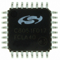
C8051F017-GQ Silicon Laboratories Inc, C8051F017-GQ Datasheet - Page 53

C8051F017-GQ
Manufacturer Part Number
C8051F017-GQ
Description
IC 8051 MCU 32K FLASH 32LQFP
Manufacturer
Silicon Laboratories Inc
Series
C8051F01xr
Specifications of C8051F017-GQ
Program Memory Type
FLASH
Program Memory Size
32KB (32K x 8)
Package / Case
32-LQFP
Core Processor
8051
Core Size
8-Bit
Speed
25MHz
Connectivity
SMBus (2-Wire/I²C), SPI, UART/USART
Peripherals
Brown-out Detect/Reset, POR, PWM, Temp Sensor, WDT
Number Of I /o
8
Ram Size
2.25K x 8
Voltage - Supply (vcc/vdd)
2.7 V ~ 3.6 V
Data Converters
A/D 4x10b; D/A 2x12b
Oscillator Type
Internal
Operating Temperature
-40°C ~ 85°C
Processor Series
C8051F0x
Core
8051
Data Bus Width
8 bit
Data Ram Size
2.25 KB
Interface Type
I2C/SMBus/SPI/UART
Maximum Clock Frequency
25 MHz
Number Of Programmable I/os
8
Number Of Timers
4
Operating Supply Voltage
2.7 V to 3.6 V
Maximum Operating Temperature
+ 85 C
Mounting Style
SMD/SMT
3rd Party Development Tools
PK51, CA51, A51, ULINK2
Development Tools By Supplier
C8051F005DK
Minimum Operating Temperature
- 40 C
On-chip Adc
4-ch x 10-bit
On-chip Dac
2-ch x 12-bit
No. Of I/o's
8
Ram Memory Size
256Byte
Cpu Speed
25MHz
No. Of Timers
4
No. Of Pwm Channels
5
Rohs Compliant
Yes
Lead Free Status / RoHS Status
Lead free / RoHS Compliant
Eeprom Size
-
Lead Free Status / Rohs Status
Lead free / RoHS Compliant
Other names
336-1196
Available stocks
Company
Part Number
Manufacturer
Quantity
Price
Company:
Part Number:
C8051F017-GQ
Manufacturer:
Silicon Labs
Quantity:
135
Company:
Part Number:
C8051F017-GQ
Manufacturer:
Silicon Laboratories Inc
Quantity:
10 000
Company:
Part Number:
C8051F017-GQR
Manufacturer:
Silicon Laboratories Inc
Quantity:
10 000
53
Bits7-0: DAC1 Data Word Most Significant Byte.
Bits7-0: DAC1 Data Word Least Significant Byte.
Bit7:
Bits6-3: UNUSED. Read = 0000b; Write = don’t care
Bits2-0: DAC1DF2-0: DAC1 Data Format Bits
C8051F000/1/2/5/6/7
C8051F010/1/2/5/6/7
DAC1EN
MSB
R/W
R/W
R/W
Bit7
Bit7
Bit7
DAC1EN: DAC1 Enable Bit
0: DAC1 Disabled. DAC1 Output pin is disabled; DAC1 is in low power shutdown mode.
1: DAC1 Enabled. DAC1 Output is pin active; DAC1 is operational.
000: The most significant nybble of the DAC1 Data Word is in DAC1H[3:0], while the least
001: The most significant 5-bits of the DAC1 Data Word is in DAC1H[4:0], while the least
010: The most significant 6-bits of the DAC1 Data Word is in DAC1H[5:0], while the least
011: The most significant 7-bits of the DAC1 Data Word is in DAC1H[6:0], while the least
1xx: The most significant byte of the DAC1 Data Word is in DAC1H, while the least
MSB
significant byte is in DAC1L.
significant 7-bits is in DAC1L[7:1].
significant 6-bits is in DAC1L[7:2].
significant 5-bits is in DAC1L[7:3].
significant nybble is in DAC1L[7:4].
MSB
R/W
R/W
R/W
Bit6
Bit6
Bit6
-
MSB
DAC1H
DAC1H
DAC1H
DAC1H
DAC1H
Figure 7.5. DAC1H: DAC1 High Byte Register
Figure 7.7. DAC1CN: DAC1 Control Register
Figure 7.6. DAC1L: DAC1 Low Byte Register
MSB
R/W
R/W
R/W
Bit5
Bit5
Bit5
-
R/W
R/W
R/W
Bit4
Bit4
Bit4
-
Rev. 1.7
R/W
R/W
R/W
Bit3
Bit3
Bit3
-
DAC1DF2
R/W
R/W
R/W
Bit2
Bit2
Bit2
LSB
DAC1L
DAC1L
DAC1L
DAC1L
DAC1L
LSB
DAC1DF1
R/W
R/W
R/W
Bit1
Bit1
Bit1
LSB
LSB
DAC1DF0
R/W
R/W
R/W
Bit0
Bit0
Bit0
LSB
00000000
00000000
00000000
SFR Address:
SFR Address:
SFR Address:
Reset Value
Reset Value
Reset Value
0xD6
0xD5
0xD7


