R5F21356CNFP#U0 Renesas Electronics America, R5F21356CNFP#U0 Datasheet - Page 339
R5F21356CNFP#U0
Manufacturer Part Number
R5F21356CNFP#U0
Description
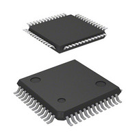
MCU 1KB FLASH 32K ROM 52-LQFP
Manufacturer
Renesas Electronics America
Series
R8C/3x/35Cr
Datasheet
1.R5F21356CNFPU0.pdf
(762 pages)
Specifications of R5F21356CNFP#U0
Core Processor
R8C
Core Size
16/32-Bit
Speed
20MHz
Connectivity
I²C, LIN, SIO, SSU, UART/USART
Peripherals
POR, PWM, Voltage Detect, WDT
Number Of I /o
47
Program Memory Size
32KB (32K x 8)
Program Memory Type
FLASH
Ram Size
2.5K x 8
Voltage - Supply (vcc/vdd)
1.8 V ~ 5.5 V
Data Converters
A/D 12x10b; D/A 2x8b
Oscillator Type
Internal
Operating Temperature
-20°C ~ 85°C
Package / Case
52-LQFP
Lead Free Status / RoHS Status
Lead free / RoHS Compliant
Eeprom Size
-
Available stocks
Company
Part Number
Manufacturer
Quantity
Price


R8C/35C Group
REJ09B0567-0100 Rev.1.00 Dec. 14, 2009
Page 306 of 725
20. Timer RD
Timer RD has 2 16-bit timers (timer RD0 and timer RD1).
20.1
Table 20.1
The count source is f1, f2, f4, f8, f32, fC2, or TRDCLK input
(bits TCK2 to TCK0 in registers TRDCR0 and TRDCR1 are set to a value from 000b
to 101b).
The count source is fOCO40M
(bits TCK2 to TCK0 in registers TRDCR0 and TRDCR1 are set to 110b).
The count source is fOCO-F
(bits TCK2 to TCK0 in registers TRDCR0 and TRDCR1 are set to 111b).
Timer RDi (i=0 or 1) has 4 I/O pins.
The operation clock of timer RD is f1, fOCO40M or fOCO-F. Table 20.1 lists the Timer RD Operation Clocks.
Figure 20.1 shows a Timer RD Block Diagram, and Table 20.2 lists Pin Configuration of Timer RD.
Timer RD has 5 modes:
• Timer mode
The following 4 modes use the output compare function.
• PWM mode
• Reset synchronous PWM mode
• Complementary PWM mode
• PWM3 mode
In the input capture function, output compare function, and PWM mode, timer RD0 and timer RD1 have the
equivalent functions, and functions or modes can be selected individually for each pin. Also, a combination of
these functions and modes can be used in timer RDi.
In reset synchronous PWM mode, complementary PWM mode, and PWM3 mode, a waveform is output with a
combination of counters and registers in timer RD0 and timer RD1.
- Input capture function
- Output compare function
Overview
Timer RD Operation Clocks
Condition
Transfer the counter value to a register with an external signal as the
trigger
(Pin output can be changed at detection)
Output pulse of any width continuously
Output three-phase waveforms (6) without sawtooth wave modulation and
dead time
Output three-phase waveforms (6) with triangular wave modulation and
dead time
Output PWM waveforms (2) with a fixed period
Detect register value matches with a counter
f1
fOCO40M
fOCO-F
Operation Clock of Timer RD
20. Timer RD
Related parts for R5F21356CNFP#U0
Image
Part Number
Description
Manufacturer
Datasheet
Request
R

Part Number:
Description:
KIT STARTER FOR M16C/29
Manufacturer:
Renesas Electronics America
Datasheet:

Part Number:
Description:
KIT STARTER FOR R8C/2D
Manufacturer:
Renesas Electronics America
Datasheet:

Part Number:
Description:
R0K33062P STARTER KIT
Manufacturer:
Renesas Electronics America
Datasheet:

Part Number:
Description:
KIT STARTER FOR R8C/23 E8A
Manufacturer:
Renesas Electronics America
Datasheet:

Part Number:
Description:
KIT STARTER FOR R8C/25
Manufacturer:
Renesas Electronics America
Datasheet:

Part Number:
Description:
KIT STARTER H8S2456 SHARPE DSPLY
Manufacturer:
Renesas Electronics America
Datasheet:

Part Number:
Description:
KIT STARTER FOR R8C38C
Manufacturer:
Renesas Electronics America
Datasheet:

Part Number:
Description:
KIT STARTER FOR R8C35C
Manufacturer:
Renesas Electronics America
Datasheet:

Part Number:
Description:
KIT STARTER FOR R8CL3AC+LCD APPS
Manufacturer:
Renesas Electronics America
Datasheet:
Part Number:
Description:
KIT STARTER FOR RX610
Manufacturer:
Renesas Electronics America
Datasheet:

Part Number:
Description:
KIT STARTER FOR R32C/118
Manufacturer:
Renesas Electronics America
Datasheet:

Part Number:
Description:
KIT DEV RSK-R8C/26-29
Manufacturer:
Renesas Electronics America
Datasheet:

Part Number:
Description:
KIT STARTER FOR SH7124
Manufacturer:
Renesas Electronics America
Datasheet:

Part Number:
Description:
KIT STARTER FOR H8SX/1622
Manufacturer:
Renesas Electronics America
Datasheet:

Part Number:
Description:
KIT DEV FOR SH7203
Manufacturer:
Renesas Electronics America
Datasheet: