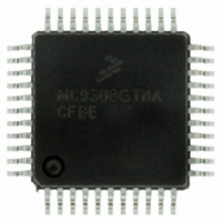
MC9S08GT8ACFBE Freescale Semiconductor, MC9S08GT8ACFBE Datasheet - Page 97

MC9S08GT8ACFBE
Manufacturer Part Number
MC9S08GT8ACFBE
Description
IC MCU 8K FLASH 1K RAM 44-QFP
Manufacturer
Freescale Semiconductor
Series
HCS08r
Datasheet
1.MC9S08GT8ACFBER.pdf
(300 pages)
Specifications of MC9S08GT8ACFBE
Core Processor
HCS08
Core Size
8-Bit
Speed
40MHz
Connectivity
I²C, SCI, SPI
Peripherals
LVD, POR, PWM, WDT
Number Of I /o
36
Program Memory Size
8KB (8K x 8)
Program Memory Type
FLASH
Ram Size
1K x 8
Voltage - Supply (vcc/vdd)
1.8 V ~ 3.6 V
Data Converters
A/D 8x10b
Oscillator Type
Internal
Operating Temperature
-40°C ~ 85°C
Package / Case
44-QFP
Processor Series
S08GT
Core
HCS08
Data Bus Width
8 bit
Data Ram Size
1 KB
Interface Type
I2C/SCI/SPI
Maximum Clock Frequency
40 MHz
Number Of Programmable I/os
36
Operating Supply Voltage
3.6 V
Maximum Operating Temperature
+ 85 C
Mounting Style
SMD/SMT
3rd Party Development Tools
EWS08
Development Tools By Supplier
M68EVB908GB60E, M68DEMO908GB60E
Minimum Operating Temperature
- 40 C
On-chip Adc
8-ch x 10-bit
For Use With
M68DEMO908GB60E - BOARD DEMO MC9S08GB60M68EVB908GB60E - BOARD EVAL FOR MC9S08GB60
Lead Free Status / RoHS Status
Lead free / RoHS Compliant
Eeprom Size
-
Lead Free Status / Rohs Status
Lead free / RoHS Compliant
Available stocks
Company
Part Number
Manufacturer
Quantity
Price
Company:
Part Number:
MC9S08GT8ACFBE
Manufacturer:
FREESCALE
Quantity:
1 600
Company:
Part Number:
MC9S08GT8ACFBE
Manufacturer:
Freescale Semiconductor
Quantity:
10 000
Company:
Part Number:
MC9S08GT8ACFBER
Manufacturer:
Freescale Semiconductor
Quantity:
10 000
- Current page: 97 of 300
- Download datasheet (2Mb)
6.5.6
Port G includes four general-purpose I/O pins that are shared with BKGD/MS function and the oscillator
or external clock pins. Port G pins used as general-purpose I/O pins are controlled by the port G data
(PTGD), data direction (PTGDD), pullup enable (PTGPE), and slew rate control (PTGSE) registers.
Port pin PTG0, while in reset, defaults to the BKGD/MS pin. After the MCU is exits reset, PTG0 can be
configured to be a general-purpose output pin. When BKGD/MS takes control of PTG0, the corresponding
PTGDD, PTGPE, and PTGPSE bits are ignored.
Port pins PTG1 and PTG2 can be configured to be oscillator or external clock pins. When the oscillator
takes control of a port G pin, the corresponding PTGD, PTGDD, PTGSE, and PTGPE bits are ignored.
Reads of PTGD will return the logic value of the corresponding pin, provided PTGDD is 0.
Freescale Semiconductor
PTGPE[3:0]
PTGD[3:0]
Reset
Reset
Field
Field
3:0
3:0
W
W
R
R
Port G Registers (PTGD, PTGPE, PTGSE, and PTGDD)
Port PTG Data Register Bits — For port G pins that are inputs, reads return the logic level on the pin. For port
G pins that are configured as outputs, reads return the last value written to this register.
Writes are latched into all bits of this register. For port G pins that are configured as outputs, the logic level is
driven out the corresponding MCU pin.
Reset forces PTGD to all 0s, but these 0s are not driven out the corresponding pins because reset also
configures all port pins as high-impedance inputs with pullups disabled.
Pullup Enable for Port G Bits — For port G pins that are inputs, these read/write control bits determine whether
internal pullup devices are enabled. For port G pins that are configured as outputs, these bits are ignored and
the internal pullup devices are disabled.
0 Internal pullup device disabled.
1 Internal pullup device enabled.
0
0
7
0
7
0
0
0
0
0
6
6
Figure 6-29. Pullup Enable for Port G (PTGPE)
Figure 6-28. Port PTG Data Register (PTGD)
Table 6-22. PTGPE Field Descriptions
Table 6-21. PTGD Field Descriptions
MC9S08GT16A/GT8A Data Sheet, Rev. 1
0
0
0
0
5
5
0
0
0
0
4
4
Description
Description
PTGPE3
PTGD3
3
0
3
0
PTGPE2
PTGD2
0
0
2
2
PTGPE1
PTGD1
0
0
1
1
Parallel Input/Output
PTGPE0
PTGD0
0
0
0
0
97
Related parts for MC9S08GT8ACFBE
Image
Part Number
Description
Manufacturer
Datasheet
Request
R
Part Number:
Description:
Manufacturer:
Freescale Semiconductor, Inc
Datasheet:
Part Number:
Description:
Manufacturer:
Freescale Semiconductor, Inc
Datasheet:
Part Number:
Description:
Manufacturer:
Freescale Semiconductor, Inc
Datasheet:
Part Number:
Description:
Manufacturer:
Freescale Semiconductor, Inc
Datasheet:
Part Number:
Description:
Manufacturer:
Freescale Semiconductor, Inc
Datasheet:
Part Number:
Description:
Manufacturer:
Freescale Semiconductor, Inc
Datasheet:
Part Number:
Description:
Manufacturer:
Freescale Semiconductor, Inc
Datasheet:
Part Number:
Description:
Manufacturer:
Freescale Semiconductor, Inc
Datasheet:
Part Number:
Description:
Manufacturer:
Freescale Semiconductor, Inc
Datasheet:
Part Number:
Description:
Manufacturer:
Freescale Semiconductor, Inc
Datasheet:
Part Number:
Description:
Manufacturer:
Freescale Semiconductor, Inc
Datasheet:
Part Number:
Description:
Manufacturer:
Freescale Semiconductor, Inc
Datasheet:
Part Number:
Description:
Manufacturer:
Freescale Semiconductor, Inc
Datasheet:
Part Number:
Description:
Manufacturer:
Freescale Semiconductor, Inc
Datasheet:
Part Number:
Description:
Manufacturer:
Freescale Semiconductor, Inc
Datasheet:


