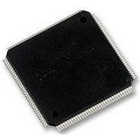
STM32F103ZET6TR STMicroelectronics, STM32F103ZET6TR Datasheet - Page 13

STM32F103ZET6TR
Manufacturer Part Number
STM32F103ZET6TR
Description
MCU 32BIT ARM 512K FLASH 100-LQF
Manufacturer
STMicroelectronics
Series
STM32r
Specifications of STM32F103ZET6TR
Core Processor
ARM® Cortex-M3™
Core Size
32-Bit
Speed
72MHz
Connectivity
CAN, I²C, IrDA, LIN, SPI, UART/USART, USB
Peripherals
DMA, Motor Control PWM, PDR, POR, PVD, PWM, Temp Sensor, WDT
Number Of I /o
112
Program Memory Size
512KB (512K x 8)
Program Memory Type
FLASH
Ram Size
64K x 8
Voltage - Supply (vcc/vdd)
2 V ~ 3.6 V
Data Converters
A/D 21x12b; D/A 2x12b
Oscillator Type
Internal
Operating Temperature
-40°C ~ 85°C
Package / Case
100-LQFP
Processor Series
STM32F103x
Core
ARM Cortex M3
Data Bus Width
32 bit
Data Ram Size
64 KB
Interface Type
CAN, I2C, SPI, USART
Maximum Clock Frequency
72 MHz
Number Of Programmable I/os
112
Number Of Timers
11
Operating Supply Voltage
2 V to 3.6 V
Maximum Operating Temperature
+ 85 C
Mounting Style
SMD/SMT
3rd Party Development Tools
EWARM, EWARM-BL, KSDK-STM32-PLUS, KSK-STM32F103ZE, MDK-ARM, RL-ARM, ULINK2
Minimum Operating Temperature
- 40 C
On-chip Adc
12 bit, 21 Channel
On-chip Dac
12 bit, 2 Channel
Cpu Family
STM32
Device Core
ARM Cortex-M3
Device Core Size
32b
Frequency (max)
72MHz
Total Internal Ram Size
64KB
# I/os (max)
112
Number Of Timers - General Purpose
8
Operating Supply Voltage (typ)
2.5/3.3V
Operating Supply Voltage (max)
3.6V
Operating Supply Voltage (min)
2V
Instruction Set Architecture
RISC
Operating Temp Range
-40C to 85C
Operating Temperature Classification
Industrial
Mounting
Surface Mount
Pin Count
144
Package Type
LQFP
For Use With
497-10030 - STARTER KIT FOR STM32497-8511 - KIT STARTER FOR STM32 512K FLASH497-6438 - BOARD EVALUTION FOR STM32 512K
Lead Free Status / RoHS Status
Lead free / RoHS Compliant
Eeprom Size
-
Lead Free Status / Rohs Status
Details
Available stocks
Company
Part Number
Manufacturer
Quantity
Price
STM32F103xC, STM32F103xD, STM32F103xE
Figure 2.
1. When the HSI is used as a PLL clock input, the maximum system clock frequency that can be achieved is
2. For the USB function to be available, both HSE and PLL must be enabled, with the CPU running at either
3. To have an ADC conversion time of 1 µs, APB2 must be at 14 MHz, 28 MHz or 56 MHz.
OSC32_OUT
OSC32_IN
OSC_OUT
64 MHz.
48 MHz or 72 MHz.
OSC_IN
MCO
Clock tree
4-16 MHz
32.768 kHz
HSE OSC
Main
Clock Output
LSE OSC
HSI RC
8 MHz
LSI RC
40 kHz
PLLSRC
MCO
x2, x3, x4
PLLMUL
HSI
..., x16
PLLXTPRE
PLL
/2
/128
LSE
LSI
/2
RTCSEL[1:0]
/2
HSE
SYSCLK
PLLCLK
HSI
Doc ID 14611 Rev 7
PLLCLK
RTCCLK
to Independent Watchdog (IWDG)
HSI
HSE
CSS
SW
SYSCLK
72 MHz
to RTC
max
IWDGCLK
Prescaler
/1, 2..512
AHB
Prescaler
Peripheral clock
enable
Peripheral clock
enable
/1, 1.5
USB
/1, 2, 4, 8, 16
TIM2,3,4,5,6,7
If (APB1 prescaler =1) x1
/1, 2, 4, 8, 16
If (APB2 prescaler =1) x1
TIM1 & 8 timers
Peripheral clock
enable
Peripheral clock
enable
/8
Prescaler
Prescaler
72 MHz max
APB2
APB1
Prescaler
/2, 4, 6, 8
Clock
/2
Enable (4 bits)
ADC
48 MHz
HSE = High Speed External clock signal
HSI = High Speed Internal clock signal
LSI = Low Speed Internal clock signal
LSE = Low Speed External clock signal
Legend:
I2S3CLK
I2S2CLK
Peripheral clock
enable
else x2
72 MHz max
else x2
36 MHz max
ADCCLK
Peripheral Clock
Peripheral Clock
Enable (20 bits)
Enable (15 bits)
USBCLK
to USB interface
Peripheral Clock
Enable (6 bits)
HCLK
to AHB bus, core,
memory and DMA
FCLK Cortex
free running clock
to I2S3
to I2S2
to Cortex System timer
Peripheral Clock
Enable (2 bit)
To SDIO AHB interface
FSMCCLK
SDIOCLK
HCLK/2
to TIM2,3,4,5,6 and 7
TIMxCLK
TIMXCLK
peripherals to APB2
PCLK1
PCLK2
to APB1
peripherals
to ADC1, 2 or 3
to FSMC
Description
to TIM1 and TIM8
to SDIO
ai14752b
13/123


