ATTINY44-15MZ Atmel, ATTINY44-15MZ Datasheet - Page 98
ATTINY44-15MZ
Manufacturer Part Number
ATTINY44-15MZ
Description
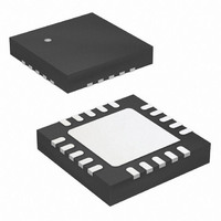
MCU AVR 4K FLASH 15MHZ 20-QFN
Manufacturer
Atmel
Series
AVR® ATtinyr
Datasheet
1.ATTINY44-15MZ.pdf
(225 pages)
Specifications of ATTINY44-15MZ
Package / Case
20-QFN Exposed Pad
Voltage - Supply (vcc/vdd)
2.7 V ~ 5.5 V
Operating Temperature
-40°C ~ 125°C
Speed
16MHz
Number Of I /o
12
Eeprom Size
256 x 8
Core Processor
AVR
Program Memory Type
FLASH
Ram Size
256 x 8
Program Memory Size
4KB (4K x 8)
Data Converters
A/D 8x10b
Oscillator Type
Internal
Peripherals
Brown-out Detect/Reset, POR, PWM, WDT
Connectivity
USI
Core Size
8-Bit
Processor Series
ATTINY4x
Core
AVR8
Data Bus Width
8 bit
Data Ram Size
256 B
Interface Type
SPI, UART
Maximum Clock Frequency
16 MHz
Number Of Programmable I/os
12
Number Of Timers
2
Maximum Operating Temperature
+ 85 C
Mounting Style
SMD/SMT
3rd Party Development Tools
EWAVR, EWAVR-BL
Development Tools By Supplier
ATAVRDRAGON, ATSTK500, ATSTK600, ATAVRISP2, ATAVRONEKIT
Minimum Operating Temperature
- 40 C
On-chip Adc
10 bit, 8 Channel
Lead Free Status / RoHS Status
Lead free / RoHS Compliant
Available stocks
Company
Part Number
Manufacturer
Quantity
Price
Company:

Part Number:
ATTINY44-15MZ
Manufacturer:
ATMEL
Quantity:
1 000
Part Number:
ATTINY44-15MZ
Manufacturer:
ATMEL/爱特梅尔
Quantity:
20 000


14.6
98
Input Capture Unit
Atmel ATtiny24/44/84 [Preliminary]
The Timer/Counter Overflow Flag (TOV1) is set according to the mode of operation selected
by the WGM13:0 bits. TOV1 can be used for generating a CPU interrupt.
The timer/counter incorporates an input capture unit that can capture external events and give
them a time stamp indicating time of occurrence. The external signal indicating an event, or
multiple events, can be applied via the ICP1 pin or, alternatively, via the analog comparator
unit. The time stamps can then be used to calculate frequency, duty cycle, and other features
of the signal applied. Alternatively, the time stamps can be used for creating a log of the
events.
The input capture unit is illustrated by the block diagram shown in
The elements of the block diagram that are not directly a part of the input capture unit are
shaded gray. The small "n" in register and bit names indicates the timer/counter number.
Figure 14-3. Input Capture Unit Block Diagram
When a change of the logic level (an event) occurs on the input capture pin (ICP1), or alterna-
tively on the analog comparator output (ACO), and this change conforms to the setting of the
edge detector, a capture will be triggered. When a capture is triggered, the 16-bit value of the
counter (TCNT1) is written to the input capture register (ICR1). The input capture flag (ICF1) is
set at the same system clock as the TCNT1 value is copied into ICR1 register. If enabled
(ICIE1 = 1), the input capture flag generates an input capture interrupt. The ICF1 flag is auto-
matically cleared when the interrupt is executed. Alternatively, the ICF1 flag can be cleared by
software by writing a logical one to its I/O bit location.
Reading the 16-bit value in the input capture register (ICR1) is done by first reading the low
byte (ICR1L) and then the high byte (ICR1H). When the low byte is read, the high byte is cop-
ied into the high byte temporary register (TEMP). When the CPU reads the ICR1H I/O
location, it will access the TEMP register.
ICPn
WRITE
ICRnH (8-bit)
TEMP (8-bit)
Comparator
Analog
ICRn (16-bit Register)
ACO*
ICRnL (8-bit)
ACIC*
DATA BUS
Canceler
ICNC
Noise
(8-bit)
TCNTnH (8-bit)
TCNTn (16-bit Counter)
Detector
ICES
Edge
Figure 14-3 on page
TCNTnL (8-bit)
ICFn (Int.Req.)
7701E–AVR–02/11
98.
Related parts for ATTINY44-15MZ
Image
Part Number
Description
Manufacturer
Datasheet
Request
R

Part Number:
Description:
Manufacturer:
Atmel Corporation
Datasheet:
Part Number:
Description:
Manufacturer:
Atmel Corporation
Datasheet:

Part Number:
Description:
IC MCU AVR 4K FLASH 20MHZ 20-QFN
Manufacturer:
Atmel
Datasheet:

Part Number:
Description:
IC MCU AVR 4K FLASH 20MHZ 14SOIC
Manufacturer:
Atmel
Datasheet:

Part Number:
Description:
MCU AVR 4KB FLASH 20MHZ 14SOIC
Manufacturer:
Atmel
Datasheet:
Part Number:
Description:
MCU AVR 4KB FLASH 20MHZ 20QFN
Manufacturer:
Atmel
Datasheet:
Part Number:
Description:
IC MCU AVR 4K FLASH 15MHZ 14SOIC
Manufacturer:
Atmel
Datasheet:

Part Number:
Description:
IC MCU AVR 4K FLASH 20MHZ 14-DIP
Manufacturer:
Atmel
Datasheet:
Part Number:
Description:
Manufacturer:
Atmel Corporation
Datasheet:
Part Number:
Description:
Microcontrollers (MCU) 512B FL 32B SRAM TIMER ATTINY4 12MHz
Manufacturer:
Atmel
Part Number:
Description:
IC MCU AVR 512B FLASH SOT-23-6
Manufacturer:
Atmel
Datasheet:

Part Number:
Description:
IC MCU AVR 512B FLASH SOT-23-6
Manufacturer:
Atmel
Datasheet: