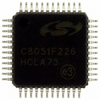
C8051F226-GQ Silicon Laboratories Inc, C8051F226-GQ Datasheet - Page 66

C8051F226-GQ
Manufacturer Part Number
C8051F226-GQ
Description
IC 8051 MCU 8K FLASH 48TQFP
Manufacturer
Silicon Laboratories Inc
Series
C8051F2xxr
Specifications of C8051F226-GQ
Program Memory Type
FLASH
Program Memory Size
8KB (8K x 8)
Package / Case
48-TQFP, 48-VQFP
Core Processor
8051
Core Size
8-Bit
Speed
25MHz
Connectivity
SPI, UART/USART
Peripherals
Brown-out Detect/Reset, POR, WDT
Number Of I /o
32
Ram Size
1.25K x 8
Voltage - Supply (vcc/vdd)
2.7 V ~ 3.6 V
Data Converters
A/D 32x8b
Oscillator Type
Internal
Operating Temperature
-40°C ~ 85°C
Processor Series
C8051F2x
Core
8051
Data Bus Width
8 bit
Data Ram Size
1.25 KB
Interface Type
SPI/UART
Maximum Clock Frequency
25 MHz
Number Of Programmable I/os
32
Number Of Timers
3
Operating Supply Voltage
2.7 V to 3.6 V
Maximum Operating Temperature
+ 85 C
Mounting Style
SMD/SMT
3rd Party Development Tools
PK51, CA51, A51, ULINK2
Development Tools By Supplier
C8051F226DK
Minimum Operating Temperature
- 40 C
On-chip Adc
32-ch x 8-bit
Package
48TQFP
Device Core
8051
Family Name
C8051F2xx
Maximum Speed
25 MHz
Lead Free Status / RoHS Status
Lead free / RoHS Compliant
For Use With
336-1241 - DEV KIT F220/221/226/230/231/236
Eeprom Size
-
Lead Free Status / Rohs Status
Lead free / RoHS Compliant
Other names
336-1240
Available stocks
Company
Part Number
Manufacturer
Quantity
Price
Company:
Part Number:
C8051F226-GQ
Manufacturer:
SILICON
Quantity:
10
Company:
Part Number:
C8051F226-GQ
Manufacturer:
Silicon Laboratories Inc
Quantity:
10 000
Company:
Part Number:
C8051F226-GQR
Manufacturer:
Silicon Laboratories Inc
Quantity:
10 000
C8051F2xx
9.2.3. General Purpose Registers
The lower 32 bytes of data memory, locations 0x00 through 0x1F, may be addressed as four banks of gen-
eral-purpose registers. Each bank consists of eight byte-wide registers designated R0 through R7. Only
one of these banks may be enabled at a time. Two bits in the program status word, RS0 (PSW.3) and RS1
(PSW.4), select the active register bank (see description of the PSW in SFR Definition 9.4). This allows
fast context switching when entering subroutines and interrupt service routines. Indirect addressing
modes use registers R0 and R1 as index registers.
9.2.4. Bit Addressable Locations
In addition to direct access to data memory organized as bytes, the sixteen data memory locations at 0x20
through 0x2F are also accessible as 128 individually addressable bits. Each bit has a bit address from
0x00 to 0x7F. Bit 0 of the byte at 0x20 has bit address 0x00 while bit 7 of the byte at 0x20 has bit address
0x07. Bit 7 of the byte at 0x2F has bit address 0x7F. A bit access is distinguished from a full byte access
by the type of instruction used (bit source or destination operands as opposed to a byte source or destina-
tion).
The MCS-51™ assembly language allows an alternate notation for bit addressing of the form XX.B where
XX is the byte address and B is the bit position within the byte. For example, the instruction:
moves the Boolean value at 0x13 (bit 3 of the byte at location 0x22) into the user Carry flag.
66
0x1DFF
0x1FFF
0x207F
0x1E00
0x2000
0x0000
MOV
PROGRAM MEMORY
Programmable in 512
128 Byte ISP FLASH
C, 22h.3
Byte Sectors)
RESERVED
(In-System
FLASH
Figure 9.2. Memory Map
0x3FF
0x000
0xFF
0x7F
0x2F
0x1F
0x80
0x30
0x20
0x00
Rev. 1.6
(Indirect Addressing
(Direct and Indirect
General Purpose
Upper 128 RAM
Bit Addressable
Addressing)
1024 Byte
Registers
XRAM
Only)
DATA MEMORY
(Direct Addressing Only)
(C8051F226/236/206 only)
Special Function
External Data Memory
Lower 128 RAM
(Direct and Indirect
Addressing)
Register's
Mapped into
Space


