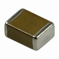
1812SC103KAT1A AVX Corporation, 1812SC103KAT1A Datasheet - Page 17

1812SC103KAT1A
Manufacturer Part Number
1812SC103KAT1A
Description
CAP CER 10000PF 1500V X7R 1812
Manufacturer
AVX Corporation
Specifications of 1812SC103KAT1A
Capacitance
10000pF
Package / Case
1812 (4532 Metric)
Voltage - Rated
1500V (1.5kV)
Tolerance
±10%
Temperature Coefficient
X7R
Mounting Type
Surface Mount, MLCC
Operating Temperature
-55°C ~ 125°C
Features
High Voltage
Applications
General Purpose
Size / Dimension
0.177" L x 0.126" W (4.50mm x 3.20mm)
Thickness
2.54mm Max
Tolerance (+ Or -)
10%
Voltage
1500VDC
Temp Coeff (dielectric)
X7R
Operating Temp Range
-55C to 125C
Mounting Style
Surface Mount
Construction
SMT Chip
Case Style
Ceramic Chip
Failure Rate
Not Required
Wire Form
Not Required
Product Length (mm)
4.5mm
Product Depth (mm)
3.2mm
Product Height (mm)
2.54mm
Product Diameter (mm)
Not Requiredmm
Capacitor Application
High Voltage
Dielectric Characteristic
X7R
Capacitance Tolerance
± 10%
Voltage Rating
1500VDC
Capacitor Case Style
1812
No. Of Pins
2
Rohs Compliant
Yes
Case Size
1812
Material, Element
Ceramic
Special Features
High Voltage
Termination
SMT
Voltage, Rating
1500 VDC
Lead Free Status / RoHS Status
Lead free / RoHS Compliant
Ratings
-
Lead Spacing
-
Lead Free Status / Rohs Status
RoHS Compliant part
Other names
1812SC103KAT1A
478-4735-2
478-4735-2
Surface Mounting Guide
MLC Chip Capacitors
and a target figure 2°C/second is recommended. Although
an 80°C to 120°C temperature differential is preferred,
recent developments allow a temperature differential
between the component surface and the soldering temper-
ature of 150°C (Maximum) for capacitors of 1210 size and
below with a maximum thickness of 1.25mm. The user is
cautioned that the risk of thermal shock increases as chip
size or temperature differential increases.
Soldering
Mildly activated rosin fluxes are preferred. The minimum
amount of solder to give a good joint should be used.
Excessive solder can lead to damage from the stresses
caused by the difference in coefficients of expansion
between solder, chip and substrate. AVX terminations are
suitable for all wave and reflow soldering systems. If hand
soldering cannot be avoided, the preferred technique is the
utilization of hot air soldering tools.
Cooling
Natural cooling in air is preferred, as this minimizes stresses
within the soldered joint. When forced air cooling is used,
cooling rate should not exceed 4°C/second. Quenching
is not recommended but if used, maximum temperature
differentials should be observed according to the preheat
conditions above.
Cleaning
Flux residues may be hygroscopic or acidic and must be
removed. AVX MLC capacitors are acceptable for use with
all of the solvents described in the specifications MIL-STD-
202 and EIA-RS-198. Alcohol based solvents are acceptable
and properly controlled water cleaning systems are also
acceptable. Many other solvents have been proven successful,
and most solvents that are acceptable to other components
on circuit assemblies are equally acceptable for use with
ceramic capacitors.
72
Angled crack between bottom of device to top of solder joint.
POST SOLDER HANDLING
Once SMP components are soldered to the board, any
bending or flexure of the PCB applies stresses to the sol-
dered joints of the components. For leaded devices, the
stresses are absorbed by the compliancy of the metal leads
and generally don’t result in problems unless the stress is
large enough to fracture the soldered connection.
Ceramic capacitors are more susceptible to such stress
because they don’t have compliant leads and are brittle in
nature. The most frequent failure mode is low DC resistance
or short circuit. The second failure mode is significant loss
of capacitance due to severing of contact between sets of
the internal electrodes.
Cracks caused by mechanical flexure are very easily identi-
fied and generally take one of the following two general
forms:
Mechanical cracks are often hidden underneath the termi-
nation and are difficult to see externally. However, if one end
termination falls off during the removal process from PCB,
this is one indication that the cause of failure was excessive
mechanical stress due to board warping.
Fracture from top of device to bottom of device.
Type A:
Type B:


