KIT33291DWEVB Freescale Semiconductor, KIT33291DWEVB Datasheet - Page 6
KIT33291DWEVB
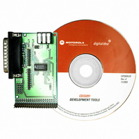
Manufacturer Part Number
KIT33291DWEVB
Description
KIT EVAL FOR MC33291 SMART SW
Manufacturer
Freescale Semiconductor
Datasheet
1.MCZ33291EGR2.pdf
(27 pages)
Specifications of KIT33291DWEVB
Main Purpose
Power Management, Low Side Driver (Internal FET)
Embedded
No
Utilized Ic / Part
MC33291
Primary Attributes
8 Channel Internal Switch
Secondary Attributes
Overvoltage, Short-Circuit & Thermal Protection
Lead Free Status / RoHS Status
Contains lead / RoHS non-compliant


6
33291
Table 4. Static Electrical Characteristics
Typical values noted reflect the approximate value with V
ELECTRICAL CHARACTERISTICS
STATIC ELECTRICAL CHARACTERISTICS
POWER INPUT
POWER OUTPUT
Notes
Supply Voltage Range
Supply Current (All Outputs ON, I
Sleep State Supply Current at
Sleep State Output Leakage Current (Per Output,
Overvoltage Shutdown
Overvoltage Shutdown Hysteresis
Logic Supply Voltage
Logic Supply Current
Logic Supply Undervoltage Lockout Threshold
Drain-to-Source ON Resistance (I
Drain-to-Source ON Resistance (I
Output Self-Limiting Current
Output Fault Detect Threshold
16.
17.
18.
19.
20.
Characteristics noted under conditions 4.5 V V
RST
RST
V
V
V
V
V
V
Outputs Programmed ON, V
Output Programmed OFF
Quasi-Functional
Fully Operational
PWR
PWR
PWR
PWR
PWR
PWR
SPI inputs and outputs operational. Fault status reporting may not be fully operational within this voltage range. Outputs remain
operational somewhat below this V
establish their instructed state following a V
This parameter is guaranteed by design, but it is not production tested.
Measured with the
Device incorporates a power-ON reset function. For V
reset and all outputs are disabled.
Output Fault Detect Threshold with outputs programmed OFF. Output fault detect thresholds are the same for output opens and shorts.
= 9.0 V
= 13 V
= 9.0 V
= 13 V
0.7 V
0.5 V
= 5.5 V
= 5.5 V
DD
(16)
(18)
RST
Characteristic
pin held at a logic high state. Outputs can be OFF or ON or in any combination thereof.
RST
(20)
OUT
OUT
OUT
OUT
(17)
= 0.6 V
0.2 V
= 0.5 A)
= 0.5 A, T
= 0.5 A, T
STATIC ELECTRICAL CHARACTERISTICS
PWR
DD
DD
and/or V
range, but R
(19)
J
J
PWR
- 25 C)
- 150 C)
RST
DD
interruption as long as V
DD
= 0 V)
< 0.5 V
DS(ON)
DD
5.5 V, 9.0 V V
BAT
less than the Undervoltage Lockout Threshold voltage, all data registers are
will increase, causing power dissipation to increase. Outputs will re-
= 13 V, T
A
PWR
V
V
V
V
= 25 C.
V
V
I
I
DD
I
Symbol
PWR(ON)
RDS(ON)
RDS(ON)
OUT(LIM)
PWR(SS)
DD
PWR(QF)
PWR(FO)
PWR(ON)
OUTth(F)
OV(HYS)
V
V
I
remains non-interrupted.
DD
(UVLO)
OV
DD
16 V, -40 C T
Min
5.5
9.0
0.2
4.5
2.5
1.0
2.5
28
–
–
–
–
–
–
–
–
–
–
–
Analog Integrated Circuit Device Data
A
125 C, unless otherwise noted.
0.55
Typ
1.0
1.0
1.0
0.8
1.0
0.6
1.2
1.0
2.0
3.0
32
–
–
–
–
–
–
–
Freescale Semiconductor
Max
26.5
9.0
2.0
2.5
2.5
1.5
5.5
4.0
3.5
2.0
1.2
1.0
3.0
1.6
1.2
3.0
3.5
36
25
Unit
mA
mA
V
V
V
V
V
A
V
A
A
A
Related parts for KIT33291DWEVB
Image
Part Number
Description
Manufacturer
Datasheet
Request
R

Part Number:
Description:
Manufacturer:
Freescale Semiconductor, Inc
Datasheet:
Part Number:
Description:
Manufacturer:
Freescale Semiconductor, Inc
Datasheet:
Part Number:
Description:
Manufacturer:
Freescale Semiconductor, Inc
Datasheet:
Part Number:
Description:
Manufacturer:
Freescale Semiconductor, Inc
Datasheet:
Part Number:
Description:
Manufacturer:
Freescale Semiconductor, Inc
Datasheet:
Part Number:
Description:
Manufacturer:
Freescale Semiconductor, Inc
Datasheet:
Part Number:
Description:
Manufacturer:
Freescale Semiconductor, Inc
Datasheet:
Part Number:
Description:
Manufacturer:
Freescale Semiconductor, Inc
Datasheet:
Part Number:
Description:
Manufacturer:
Freescale Semiconductor, Inc
Datasheet:
Part Number:
Description:
Manufacturer:
Freescale Semiconductor, Inc
Datasheet:
Part Number:
Description:
Manufacturer:
Freescale Semiconductor, Inc
Datasheet:
Part Number:
Description:
Manufacturer:
Freescale Semiconductor, Inc
Datasheet:
Part Number:
Description:
Manufacturer:
Freescale Semiconductor, Inc
Datasheet:
Part Number:
Description:
Manufacturer:
Freescale Semiconductor, Inc
Datasheet:
Part Number:
Description:
Manufacturer:
Freescale Semiconductor, Inc
Datasheet: