DSP56309EVM Freescale Semiconductor, DSP56309EVM Datasheet - Page 12
DSP56309EVM
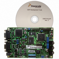
Manufacturer Part Number
DSP56309EVM
Description
KIT EVALUATION FOR XC56309
Manufacturer
Freescale Semiconductor
Type
DSPr
Specifications of DSP56309EVM
Contents
Module Board, Installation Guide, Power Supply, Cable, Software and more
Description/function
Audio DSPs
Product
Audio Modules
For Use With/related Products
DSP56309
Lead Free Status / RoHS Status
Contains lead / RoHS non-compliant


Flash Memory Programming Code Description
;----------------------------------------------------------------------------
; delay_20m --
; 21.0 ms of delay guarantees that the write cycle has finished.
; Icycles for a 98.304 MHz clock. (10.17 ns/Instruction_cycle)
; The Write Cycle Time is 20ms, so we just wait long enough here for the
; write cycle to have started AND finished...
delay_20m
_l1
;----------------------------------------------------------------------------
6.1
The main code starts with its own I/O register equates for the PLL and program bus registers (i.e it does
not use an ioequ include file) so that the codec code file can use the I/O register equate include file without
conflicts in the project. The main code also includes equates for the AAR1 and BCR control register
values. The Flash memory programming code is located at the top of the internal program memory so that
the user code can be placed in the low program memory (and use the default interrupt vector locations if
needed). See
instructions.
The first two move instructions after the main_flash label define the location of the first word of the user
code and the number of 24-bit words in the user code. The codec programming code starts at location
p:0x100 and is a little less than 0x100 words long. These values are used in the bootloader code and must
be modified if the user code is changed.
The next instructions in the main code program the PLL control register(s) using conditional assembly
directives. See
instructions. Then the main code programs the external memory interface control registers (AAR1 and
BCR) to enable access to the Flash memory. The main code also calculates number of Flash memory
sectors that are needed to contain the user code.
After the initialization, the main code uses the Flash memory write routine to write the bootloader code to
the first sector of the Flash memory. Then the main code uses the Flash memory write routine to write the
user code to the Flash memory starting at the second sector.
The main code ends at a debug instruction that passes control of the DSP to the debugger so that you know
when the code is complete.
6.2
The bootloader code is loaded by the main code to the first sector of the Flash memory. The bootloader
transfers the user code from the Flash memory (starting at the second sector of the Flash memory) to the
DSP internal program memory and then the bootloader code jumps to the beginning of the user code. As
12
Bootloader Code
bsr
rts
dor
move
rep
nop
rts
end
Main Code
Section 3.3.1, “Flash Memory Programming Code Device Define
Section 3.3.1, “Flash Memory Programming Code Device Define
main_flash
<delay_20m
#280,_l1
#7374,x0
x0
Using Symphony™ Studio with the DSP563xxEVM, Rev. 0
; wait 20 ms to finish program cycle
; 280 x 7374 x 27.13ns = 21.0 ms
for more detail of these
for more detail of these
Freescale Semiconductor
Related parts for DSP56309EVM
Image
Part Number
Description
Manufacturer
Datasheet
Request
R

Part Number:
Description:
Manufacturer:
Freescale Semiconductor, Inc
Datasheet:
Part Number:
Description:
Manufacturer:
Freescale Semiconductor, Inc
Datasheet:
Part Number:
Description:
Manufacturer:
Freescale Semiconductor, Inc
Datasheet:
Part Number:
Description:
Manufacturer:
Freescale Semiconductor, Inc
Datasheet:
Part Number:
Description:
Manufacturer:
Freescale Semiconductor, Inc
Datasheet:
Part Number:
Description:
Manufacturer:
Freescale Semiconductor, Inc
Datasheet:
Part Number:
Description:
Manufacturer:
Freescale Semiconductor, Inc
Datasheet:
Part Number:
Description:
Manufacturer:
Freescale Semiconductor, Inc
Datasheet:
Part Number:
Description:
Manufacturer:
Freescale Semiconductor, Inc
Datasheet:
Part Number:
Description:
Manufacturer:
Freescale Semiconductor, Inc
Datasheet:
Part Number:
Description:
Manufacturer:
Freescale Semiconductor, Inc
Datasheet:
Part Number:
Description:
Manufacturer:
Freescale Semiconductor, Inc
Datasheet:
Part Number:
Description:
Manufacturer:
Freescale Semiconductor, Inc
Datasheet:
Part Number:
Description:
Manufacturer:
Freescale Semiconductor, Inc
Datasheet:
Part Number:
Description:
Manufacturer:
Freescale Semiconductor, Inc
Datasheet: