CY3220LINBUS-RD Cypress Semiconductor Corp, CY3220LINBUS-RD Datasheet - Page 35
CY3220LINBUS-RD
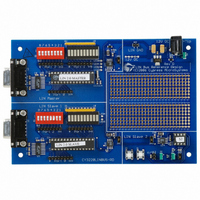
Manufacturer Part Number
CY3220LINBUS-RD
Description
KIT REF DESIGN LIN BUS
Manufacturer
Cypress Semiconductor Corp
Series
PSoC®r
Datasheet
1.CY3220LINBUS-RD.pdf
(64 pages)
Specifications of CY3220LINBUS-RD
Main Purpose
Interface, LIN
Embedded
Yes, MCU, 8-Bit
Utilized Ic / Part
CY8C27143, CY8C27443
Processor To Be Evaluated
CY8C27143-24PXI and CY8C27443-24PXI
Interface Type
RS-232
Lead Free Status / RoHS Status
Contains lead / RoHS non-compliant
Lead Free Status / RoHS Status
Lead free / RoHS Compliant, Contains lead / RoHS non-compliant
Other names
428-1926


LIN Bus 2.0 Reference Design
E. Wait For Falling Edge 1: When the first falling edge of
F. Wait For Falling Edge 2: When the second falling edge
G. Wait For Falling Edge 3: When the third falling edge of
H. Wait For Falling Edge 4: When the fourth falling edge of
4.3.3
The synchro timer interrupt has two functions.
■
October 25, 2006
and backed up. The state machine is updated as “Wait
For Falling Edge 1.”
the synch byte is detected, this state is entered. Here the
compare register of the timer is read, and the difference
between the current value and the value on the start bit
of the synch byte is found. This equals two bit times.
Then two more values are calculated from the two bit
times that are +6.25% of the measured two bit times.
These values are used to compare the two bit times
measured during the second, third and fourth falling
edges of the synch field. This comparison is to make
sure that a 0x55 is transmitted as a synch field. Any
other value transmitted as a synch field will not be within
the limits of the two bit times and the break/synch field
will be considered invalid. After this, the state machine is
updated to “Wait For Falling Edge 2.”
of the synch byte is detected, this state is entered. Here,
the time difference between the current falling edge and
the previous edge is calculated and compared with the
minimum and maximum two bit-time values calculated
during the previous state. If the value is within the limits,
the state is updated to “Wait For Falling Edge 3,” else,
the synchro reception variables are all reset and the
firmware gets ready to detect a new break/synch field.
the synch byte is detected, this state is entered. Here,
the time difference between the current falling edge and
the previous edge is calculated and compared with the
minimum and maximum two bit-time values calculated
during the first falling edge. If the value is within the lim-
its, the state is updated to “Wait For Falling Edge 4,”
else, the synchro reception variables are all reset and
the firmware gets ready to detect a new break/synch
field.
the synch byte is detected, this state is entered. Here,
the time difference between the current falling edge and
the previous edge is calculated and compared with the
minimum and maximum two bit-time values calculated
during the first falling edge. If the value is within the lim-
its, then the difference between the timer count value of
this falling edge and the timer count value backed up
during the start bit of the synch field is calculated. This
value is divided by eight to find out the bit time. Dividing
this further by eight gives the counter value to be loaded
to the baud rate generator. Then the bit time is multiplied
by 13 and the already stored break time is compared
with this to check if the break field is at least 13 bit times.
If this condition is satisfied, then the Data Reception
Configuration is loaded.
Bus Idle Detection: When there is no activity on the
bus, this interrupt is used to detect the bus idle timeout
and set the sleep flag. The specification says that if there
Synchro Timer Interrupt
Cypress Semiconductor – Rev. **
■
4.3.4
The synchro timeout counter interrupt is used to detect a
timeout condition during the break/synch detection state.
When a break signal is received and its length found, the
same length is used to set the timeout duration. So if a
break is not followed by the synch field within the 13 bit
times, the state machine is reset to detect a break signal
again. This timeout is also useful in the case when a slave is
switched on in the midst of a LIN frame. What happens is
the slave starts considering the data bits of the ongoing
frame as the break field. Under this condition, if the last bit of
the frame is considered by the slave as the break, then the
actual break of the next frame is treated as the first falling
edge of the synch byte, which results in that frame being
missed. In this event, this timeout resets the state machine
and correctly synchronizes the slave to the next break sig-
nal.
4.3.5
When a valid break/synch field is detected and the bit rate
calculations are done, the Data Reception Configuration is
loaded and the RX8 interrupt is enabled. Any data received
on the bus generates an interrupt and the received data is
processed inside this ISR. There are three states inside this
ISR.
■
■
is no activity on the bus for four seconds, the slaves
enter sleep state.
Break/Synch Timeout: When break/synch detection is
taking place, this interrupt is used to timeout the opera-
tion, in case the break/synch field does not complete. If
this timeout were not provided, the firmware would enter
an infinite loop waiting for the break/synch to complete.
Receiving and Decoding the Protected ID: The first
data received after the break/synch field is the protected
ID. When the protected ID is received, the ExtractID
function is called to check if the protected ID is present in
the ID table. This function parses through the ID table
present in the E2PROM area in the Flash. If it finds the
ID in the table, it updates the related parameters includ-
ing data count, buffer pointer, and data transfer direction
(master to slave or slave to master). It also checks if the
received protected ID is a master request or a slave
response ID. If it is either of these, then it initializes the
proper variables to carry out these operations.
Processing Received Data: When all the data indicated
by the data counter have been received, the received
data is processed. First, the checksum of the received
data is checked. If the protected ID is greater than or
equal to 60 (0x3C), classic checksum is used. For all
other IDs, extended checksum is used. If there is an
error in checksum, then proper error bits are set and the
whole data is discarded. If the checksum matches, then
the received data is transferred to the corresponding
buffer pointed to by the buffer pointer variable. Then
proper bits are set to indicate a successful transfer. If the
protected ID is a master request, the master request is
processed. When all these operations are completed,
Synchro Timeout Interrupt
RX Interrupt
4. Slave Design IP
33
Related parts for CY3220LINBUS-RD
Image
Part Number
Description
Manufacturer
Datasheet
Request
R

Part Number:
Description:
KIT DEMO PSOC CAPSENSE
Manufacturer:
Cypress Semiconductor Corp
Datasheet:

Part Number:
Description:
KIT DEMO PSOC CAPSENSE SLIDE
Manufacturer:
Cypress Semiconductor Corp

Part Number:
Description:
Manufacturer:
Cypress Semiconductor Corp
Datasheet:
Part Number:
Description:
Manufacturer:
Cypress Semiconductor Corp
Datasheet:
Part Number:
Description:
Manufacturer:
Cypress Semiconductor Corp
Datasheet:
Part Number:
Description:
Manufacturer:
Cypress Semiconductor Corp
Datasheet:
Part Number:
Description:
Manufacturer:
Cypress Semiconductor Corp
Datasheet: