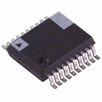
ADE7761AARS-REF Analog Devices Inc, ADE7761AARS-REF Datasheet - Page 12

ADE7761AARS-REF
Manufacturer Part Number
ADE7761AARS-REF
Description
IC DETECTOR ENERGY METER 20-SSOP
Manufacturer
Analog Devices Inc
Datasheet
1.ADE7761AARSZ-RL.pdf
(24 pages)
Specifications of ADE7761AARS-REF
Lead Free Status / RoHS Status
Contains lead / RoHS non-compliant
ADE7761A
The differential voltage MISCAL − V
to a common mode (usually AGND). The analog inputs of the
ADE7761A can be driven with common-mode voltages of up
to 100 mV with respect to AGND. However, best results are
achieved using a common mode equal to AGND.
Typical Connection Diagrams
Figure 15 shows a typical connection diagram for Channel V1.
The analog inputs are used to monitor both the phase and
neutral currents. Because of the large potential difference
between the phase and neutral, two current transformers (CTs)
must be used to provide the isolation. Note that both CTs are
referenced to analog ground (AGND); therefore, the common-
mode voltage is 0 V. The CT turns ratio and burden resistor
(RB) are selected to give a peak differential voltage of
±660 mV/gain.
Figure 16 shows two typical connections for Channel V2.
The first option uses a potential transformer (PT) to provide
complete isolation from the main voltage. In the second option,
the ADE7761A is biased around the neutral wire, and a resistor
divider is used to provide a voltage signal that is proportional to
the line voltage. Adjusting the ratio of RA and RB + VR is a
convenient way to carry out a gain calibration on the meter.
Figure 17 shows a typical connection for the MISCAL input.
The voltage reference input (REF
to set the MISCAL voltage.
IP
IN
1
RB + VR = RF.
AGND
Figure 15. Typical Connection for Channel 1
Figure 16. Typical Connection for Channel 2
RA
CT
CT
1
RB
VR
1
1
RB
RB
AGND
±660mV
±660mV
±660mV
C
GAIN
GAIN
F
R
R
F
F
R
R
R
IN/OUT
F
F
F
C
C
C
F
F
T
2N
) is used as a dc reference
C
C
must be referenced
V
V
V
V
F
F
2P
2N
2P
2N
V
V
V
1A
1N
1B
Rev. 0 | Page 12 of 24
Adjusting the level of MISCAL to calibrate the meter in missing
neutral mode can be done by changing the ratio of RC and RD
+ VR1. When the internal reference is used, the values of RC,
RD, and VR1 must be chosen to limit the current sourced by
the internal reference sourcing current to below the specified
20 μA. Therefore, because V
VR1 > 600 kΩ.
INTERNAL OSCILLATOR
The nominal internal oscillator frequency is 450 kHz when
used with the recommended R
between RCLKIN and DGND (see Figure 18).
The internal oscillator frequency is inversely proportional to the
value of this resistor. Although the internal oscillator operates
when used with an R
it is recommended to choose a value within the range of the
nominal value.
The output frequencies on CF, F1, and F2 are directly propor-
tional to the internal oscillator frequency; therefore, the resistor
R
tolerance resistor limits the variation of the internal oscillator
frequency. A small variation of the clock frequency and
consequently of the output frequencies from meter to meter
contributes to a smaller calibration range of the meter.
A low temperature drift resistor directly limits the variation of
the internal clock frequency over temperature. The stability of
the meter to external variation is then better ensured by design.
OSC
must have a low tolerance and low temperature drift. A low
REFERENCE
ADE7761A
REF
2.5V
IN/OUT
Figure 17. Typical Connection for MISCAL
Figure 18. Internal Oscillator Connection
3kΩ
REF
RC
VR1
IN/OUT
RD
9
OSC
resistor value between 5 kΩ and 12 kΩ,
OSCILLATOR
R
REF
INTERNAL
OSC
C
F
OSC
14
internal = 2.5 V, RC + RD +
RCLKIN
R
F
resistor value of 6.2 kΩ
C
F
MISCAL
V
2N
17
DGND


