AD8364-EVAL-2140 Analog Devices Inc, AD8364-EVAL-2140 Datasheet - Page 20
AD8364-EVAL-2140
Manufacturer Part Number
AD8364-EVAL-2140
Description
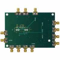
BOARD EVAL AD8364 2140MHZ
Manufacturer
Analog Devices Inc
Datasheet
1.AD8364-EVAL-2140.pdf
(48 pages)
Specifications of AD8364-EVAL-2140
Module/board Type
Evaluation Board
For Use With/related Products
AD8364 2.140GHz only
Lead Free Status / RoHS Status
Contains lead / RoHS non-compliant


AD8364
TEMPERATURE SENSOR INTERFACE
The AD8364 provides a temperature sensor output capable of
driving about 1.6 mA. A 330 Ω-equivalent internal resistance is
connected from TEMP to COMR to provide current sink
capability. The temperature scaling factor of the output voltage is
approximately 2 mV/°C. The typical absolute voltage at 25°C is
about 620 mV.
VREF INTERFACE
An internal voltage reference is provided to the user at Pin VREF.
The VREF voltage is a temperature stable 2.5 V reference that
can drive about 18 mA. An 830 Ω equivalent internal resistance
is connected from VREF to ACOM for 3 mA sink capability.
INTERNAL
INTERNAL
VOLTAGE
Figure 53. TEMP Interface Simplified Schematic
VPTAT
Figure 54. VREF Interface Simplified Schematic
COMR
COMR
VPSR
VPSR
4kΩ
1kΩ
9kΩ
1.465kΩ
350Ω
900Ω
TEMP
V
REF
Rev. 0 | Page 20 of 48
POWER-DOWN INTERFACE
The operating and stand-by currents for the AD8364 at 25°C are
approximately 70 mA and 500 µA, respectively. The PWDN pin
is connected to an internal resistor divider made with two 42 kΩ
resistors. The divider voltage is applied to the base of an NPN
transistor to force a power-down condition when the device is
active. Typically when PWDN is pulled greater than 2 V, the
device is powered down. Figure 46 and Figure 47 show typical
response times for various RF input levels. The output reaches
to within 0.1 dB of its steady-state value in about 1.6 µs; the
reference voltage is available to full accuracy in a much shorter
time. This wake-up response vary depending on the input
coupling means and the capacitances CDEC[A, B], CHP[A, B],
and CLP[A, B].
VST[A, B] INTERFACE
The VST[A, B] interface has a high input impedance of 72 kΩ.
The voltage at VST[A, B] is converted to an internal current
used to steer the VGA gain. The VGA attenuation control is
set to 20 dB/V.
VST[A, B]
Figure 56. VST[A, B] Interface Simplified Schematic
Figure 55. PWDN Interface Simplified Schematic
PWDN
36kΩ
36kΩ
COMR
42kΩ
42kΩ
POWER DOWN
SIGNAL
ACOM
GAIN ADJUST
18.5kΩ
1.35µA/dB
Related parts for AD8364-EVAL-2140
Image
Part Number
Description
Manufacturer
Datasheet
Request
R

Part Number:
Description:
LF to 2.7GHz, Dual 60dB TruPwr™ Detector; Package: EVALUATION BOARDS; No of Pins: -; Temperature Range: Commercial
Manufacturer:
Analog Devices
Datasheet:
Part Number:
Description:
LF to 2.7GHz, Dual 60dB TruPwr Detector
Manufacturer:
Analog Devices
Datasheet:

Part Number:
Description:
±1.7g Dual-Axis IMEMS Accelerometer Evaluation Board
Manufacturer:
Analog Devices Inc
Datasheet:

Part Number:
Description:
Inertial Sensor Evaluation System
Manufacturer:
Analog Devices Inc
Datasheet:
Part Number:
Description:
Manufacturer:
Analog Devices Inc
Datasheet:
Part Number:
Description:
Manufacturer:
Analog Devices Inc
Datasheet:
Part Number:
Description:
Manufacturer:
Analog Devices Inc
Datasheet:
Part Number:
Description:
Manufacturer:
Analog Devices Inc
Datasheet:
Part Number:
Description:
Manufacturer:
Analog Devices Inc
Datasheet:
Part Number:
Description:
Manufacturer:
Analog Devices Inc
Datasheet:
Part Number:
Description:
Manufacturer:
Analog Devices Inc
Datasheet:
Part Number:
Description:
Manufacturer:
Analog Devices Inc
Datasheet:
Part Number:
Description:
Manufacturer:
Analog Devices Inc
Datasheet: