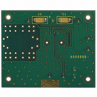
AD8230-EVAL Analog Devices Inc, AD8230-EVAL Datasheet

AD8230-EVAL
Specifications of AD8230-EVAL
Related parts for AD8230-EVAL
AD8230-EVAL Summary of contents
Page 1
... The AD8230 is versatile yet simple to use. Its auto-zeroing topology significantly minimizes the input and output transients typical of commutating or chopper instrumentation amplifiers. The AD8230 operates on ± ± +16 V) supplies and is available in an 8-lead SOIC. 1 The AD8230 can be programmed for a gain as low as 2, but the maximum input voltage is limited to approximately 750 mV ...
Page 2
... AD8230 TABLE OF CONTENTS Features .............................................................................................. 1 Applications....................................................................................... 1 General Description ......................................................................... 1 Connection Diagram ....................................................................... 1 Revision History ............................................................................... 2 Specifications..................................................................................... 3 Absolute Maximum Ratings............................................................ 5 Thermal Characteristics .............................................................. 5 ESD Caution.................................................................................. 5 Typical Performance Characteristics ............................................. 6 Theory of Operation ...................................................................... 11 Setting the Gain .......................................................................... 11 REVISION HISTORY 9/07—Rev Rev. B Changes to Features and Layout..................................................... 1 Changes to Table 1............................................................................ 3 Changes to Table 2............................................................................ 4 Changes to Layout ............................................................................ 5 Inserted Figure 13, Figure 14, and Figure 15 ...
Page 3
... TEMPERATURE RANGE Specified Performance 1 The AD8230 can operate as low However, since the differential input range is limited to approximately 750 mV, the AD8230 configured at G < 10 does not make use of the full output voltage range. 2 Gain drift is determined by the TC match of the external gain setting resistors. ...
Page 4
... TEMPERATURE RANGE Specified Performance 1 The AD8230 can operate as low However, since the differential input range is limited to approximately 750 mV, the AD8230 configured at G < 10 does not make use of the full output voltage range. 2 Gain drift is determined by the TC match of the external gain setting resistors. ...
Page 5
... THERMAL CHARACTERISTICS Specification is for device in free air SOIC. Rating ±8 V, +16 V Table 4. 304 mW Parameter 20 mA θ (4-Layer JEDEC Board) JA ±V S ±V S −65°C to +150°C ESD CAUTION −40°C to +125°C Rev Page AD8230 Value Unit 121 °C/W ...
Page 6
... AD8230 TYPICAL PERFORMANCE CHARACTERISTICS TOTAL NUMBER OF SAMPLES = 2839 FROM 3 LOTS 500 400 300 200 100 0 –9 –6 –3 0 OFFSET VOLTAGE (µV RTI) Figure 4. Offset Voltage (RTI) Distribution at ± TOTAL NUMBER OF SAMPLES = 300 FROM 3 LOTS –50 –30 –10 10 OFFSET VOLTAGE DRIFT (nV/°C) Figure 5 ...
Page 7
... Figure 14. Input Common-Mode Voltage Range vs. Output Voltage –7.9V, + –2 –4 –6 –8 –7.9V, –8V – –10 –8 Figure 15. Input Common-Mode Voltage Range vs. Output Voltage 100 Rev Page AD8230 0V, +8.4V +592mV, +8. ±8V S –812mV, +5V 0V, +5.5V +644mV, + ±5V S –652mV, –5V +800mV, –5V 0V, –5.5V +840mV, –8.2V 0V, –8.4V 0 200 400 600 ...
Page 8
... AD8230 6.8 6.6 6.4 ±8V 6.2 6.0 ±5V 5.8 5.6 5.4 –50 –30 – TEMPERATURE (°C) Figure 16. Clock Frequency vs. Temperature 1.0 0.8 0.6 0.4 0.2 0 –0.2 –0.4 0°C –0.6 –0.8 +25°C –1.0 –6 –4 –2 0 COMMON-MODE VOLTAGE (V) Figure 17. Average Input Bias Current vs. Common-Mode Voltage, − ...
Page 9
... Figure 26. 0 RTI Voltage Noise 100 160 140 120 100 0.1 Rev Page 100 1k 10k FREQUENCY (Hz) 2µV/DIV –30 – TEMPERATURE (° +1000 G = +100 FREQUENCY (kHz) Figure 27. Positive PSR vs. Frequency, RTI AD8230 100k 1s/DIV 110 130 10 ...
Page 10
... AD8230 140 120 G = +100 100 G = +1000 0.1 1 FREQUENCY (kHz) Figure 28. Negative PSR vs. Frequency, RTI +10 –2 –4 –6 –8 – Figure 29. Output Voltage Swing vs. Output Current, Rev Page ±8V –40 ° –40 ° C +125 ° ±5V S +125 ° C +125 ° ±5V S –40 ° C +125 ° ...
Page 11
... The gain amplifier conditions the updated signal stored on the hold capacitors, C SETTING THE GAIN Two external resistors set the gain of the AD8230. The gain is expressed in the following equation: GAIN AMP S ...
Page 12
... If resistors R R (3) ⎟ + − ⎟ and capacitors are used at the input of the AD8230, care should ⎠ taken to maintain close match to maximize CMRR. Rev Page value. Table 5 shows R values for various gains using Equation 4. O × V ...
Page 13
... INPUT VOLTAGE RANGE The input common-mode range of the AD8230 is rail to rail. However, the differential input voltage range is limited to approximately 750 mV. The AD8230 does not phase invert when its inputs are overdriven. INPUT PROTECTION The input voltage is limited to within 0.6 V beyond the supply rails by the internal ESD protection diodes ...
Page 14
... The common-mode 200Ω potential can be several volts, exceeding the common-mode input range of many 5 V auto-zero instrumentation amplifiers. Fortunately, the wide common-mode input voltage range of the AD8230 spans 16 V, relieving designers of having to worry about the common-mode range. Rev Page – ...
Page 15
... COPLANARITY ORDERING GUIDE Model Temperature Range 1 AD8230YRZ −40°C to +125°C 1 AD8230YRZ-REEL −40°C to +125°C AD8230YRZ-REEL7 1 −40°C to +125°C AD8230-EVAL RoHS Compliant Part. 5.00 (0.1968) 4.80 (0.1890 6.20 (0.2441) 4.00 (0.1574) 1 5.80 (0.2284) 3.80 (0.1497) 4 1.27 (0.0500) BSC 1 ...
Page 16
... AD8230 NOTES ©2004–2007 Analog Devices, Inc. All rights reserved. Trademarks and registered trademarks are the property of their respective owners. D05063-0-9/07(B) Rev Page ...


