AD9958/PCB Analog Devices Inc, AD9958/PCB Datasheet - Page 40
AD9958/PCB
Manufacturer Part Number
AD9958/PCB
Description
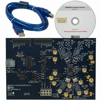
BOARD EVALUATION FOR AD9958
Manufacturer
Analog Devices Inc
Datasheet
1.AD9958BCPZ.pdf
(44 pages)
Specifications of AD9958/PCB
Design Resources
Low Jitter Sampling Clock Generator for High Performance ADCs Using AD9958/9858 and AD9515 (CN0109) Phase Coherent FSK Modulator (CN0186)
Lead Free Status / RoHS Status
Contains lead / RoHS non-compliant
Available stocks
Company
Part Number
Manufacturer
Quantity
Price
Company:

Part Number:
AD9958/PCBZ
Manufacturer:
Analog Devices Inc
Quantity:
135


AD9958
Bit
6
5
4
3:2
1
0
Function Register 2 (FR2)—Address 0x02
Two bytes are assigned to this register. The FR2 is used to control the various functions, features, and modes of the AD9958.
Table 33. Bit Descriptions for FR2
Bit
15
14
13
12
11:8
7
6
5
4
3: 2
1:0
Mnemonic
External power-down mode
SYNC_CLK disable
DAC reference power-down
Open
Manual hardware sync
Manual software sync
Mnemonic
All channels autoclear sweep
accumulator
All channels clear
sweep accumulator
All channels autoclear phase
accumulator
All channels clear phase
Accumulator
Open
Auto sync enable
Multidevice sync master enable
Multidevice sync status
Multidevice sync mask
Open
System clock offset
Description
0 = the external power-down mode is in fast recovery power-down mode (default). In this mode,
when the PWR_DWN_CTL input pin is high, the digital logic and the DAC digital logic are
powered down. The DAC bias circuitry, PLL, oscillator, and clock input circuitry are not powered
down.
1 = the external power-down mode is in full power-down mode. In this mode, when the
PWR_DWN_CTL input pin is high, all functions are powered down. This includes the DAC and PLL,
which take a significant amount of time to power up.
0 = the SYNC_CLK pin is active (default).
1 = the SYNC_CLK pin assumes a static Logic 0 state (disabled). In this state, the pin drive logic is
shut down. However, the synchronization circuitry remains active internally to maintain normal
device operation.
0 = DAC reference is enabled (default).
1 = DAC reference is powered down.
See the Synchronizing Multiple AD9958 Devices section for details.
0 = the manual hardware synchronization feature of multiple devices is inactive (default).
1 = the manual hardware synchronization feature of multiple devices is active.
1 = the manual software synchronization feature of multiple devices is active. See the
Synchronizing Multiple AD9958 Devices section for details.
Description
0 = a new delta word is applied to the input, as in normal operation, but not loaded into the
accumulator (default).
1 = this bit automatically and synchronously clears (loads 0s into) the sweep accumulator for one
cycle upon reception of the I/O_UPDATE sequence indicator on both channels.
0 = the sweep accumulator functions as normal (default).
1 = the sweep accumulator memory elements for both channels are asynchronously cleared.
0 = a new frequency tuning word is applied to the inputs of the phase accumulator, but not
loaded into the accumulator (default).
1 = this bit automatically and synchronously clears (loads 0s into) the phase accumulator for one
cycle upon receipt of the I/O update sequence indicator on both channels.
0 = the phase accumulator functions as normal (default).
1 = the phase accumulator memory elements for both channels are asynchronously cleared.
See the Synchronizing Multiple AD9958 Devices section for more details.
See the Synchronizing Multiple AD9958 Devices section for more details.
See the Synchronizing Multiple AD9958 Devices section for more details.
0 = the manual software synchronization feature of multiple devices is inactive (default).
See the Synchronizing Multiple AD9958 Devices section for more details.
See the Synchronizing Multiple AD9958 Devices section for more details.
Rev. A | Page 40 of 44
Related parts for AD9958/PCB
Image
Part Number
Description
Manufacturer
Datasheet
Request
R

Part Number:
Description:
BOARD EVALUATION FOR AD9958
Manufacturer:
Analog Devices Inc
Datasheet:


Part Number:
Description:
±1.7g Dual-Axis IMEMS Accelerometer Evaluation Board
Manufacturer:
Analog Devices Inc
Datasheet:

Part Number:
Description:
Inertial Sensor Evaluation System
Manufacturer:
Analog Devices Inc
Datasheet:
Part Number:
Description:
Manufacturer:
Analog Devices Inc
Datasheet:
Part Number:
Description:
Manufacturer:
Analog Devices Inc
Datasheet:
Part Number:
Description:
Manufacturer:
Analog Devices Inc
Datasheet:
Part Number:
Description:
Manufacturer:
Analog Devices Inc
Datasheet:
Part Number:
Description:
Manufacturer:
Analog Devices Inc
Datasheet:
Part Number:
Description:
Manufacturer:
Analog Devices Inc
Datasheet:
Part Number:
Description:
Manufacturer:
Analog Devices Inc
Datasheet:
Part Number:
Description:
Manufacturer:
Analog Devices Inc
Datasheet:
Part Number:
Description:
Manufacturer:
Analog Devices Inc
Datasheet: