AD1836A-DBRD Analog Devices Inc, AD1836A-DBRD Datasheet - Page 21
AD1836A-DBRD
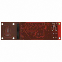
Manufacturer Part Number
AD1836A-DBRD
Description
BOARD EVAL FOR AD1836A
Manufacturer
Analog Devices Inc
Specifications of AD1836A-DBRD
Module/board Type
Evaluation Board
Lead Free Status / RoHS Status
Contains lead / RoHS non-compliant
For Use With/related Products
AD1836A
Lead Free Status / RoHS Status
Not Compliant, Contains lead / RoHS non-compliant


Table 19. ADC Control Register 3
When changing clock mode, other SPI bits that are written during the same SPI transaction may be lost. Therefore, it is recommended
that these be set separately.
Address
15, 14,
13, 12
1110
Table 20. ADC Peak Level Data Registers
Address
15, 14, 13, 12
1000 = ADC1L
1001 = ADC1R
1010 = ADC2L
1011 = ADC2R
RD/WR
11
0
Reserved
10, 9, 8
000
RD/WR
11
1
Clock Mode
7, 6
00 = 256 × f
01 = 512 × f
10 = 768 × f
Reserved
10
0
S
S
S
Function
Left Differential
I/P Select
5
0 = Differential
PGA Mode
1 = PGA/MUX
Mode (Single-
Ended Input)
Peak Level Data (10 Bits)
6 Data Bits
9:4
000000 = 0.0 dBFS
000001 = –1.0 dBFS
000010 = –2.0 dBFS
000011 = –3.0 dBFS
111100 = –60 dBFS Min
Rev. 0 | Page 21 of 24
Right
Differential
I/P Select
4
0 = Differential
PGA Mode
1 = PGA/MUX
Mode (Single-
Ended Input)
Left
MUX/PGA
Enable
3
0 = Direct
1 = MUX/PGA
4 Fixed Bits
3:0
0000
The 4 LSBs are always zero.
Left MUX
I/P Select
2
0 = I/P 0
1 = I/P 1
1
Right
MUX/PGA
Enable
0 = Direct
1 = MUX/PGA
AD1836A
Right
MUX I/P
Select
0
0 = I/P 0
1 = I/P 1
Related parts for AD1836A-DBRD
Image
Part Number
Description
Manufacturer
Datasheet
Request
R


Part Number:
Description:
±1.7g Dual-Axis IMEMS Accelerometer Evaluation Board
Manufacturer:
Analog Devices Inc
Datasheet:

Part Number:
Description:
Inertial Sensor Evaluation System
Manufacturer:
Analog Devices Inc
Datasheet:
Part Number:
Description:
Manufacturer:
Analog Devices Inc
Datasheet:
Part Number:
Description:
Manufacturer:
Analog Devices Inc
Datasheet:
Part Number:
Description:
Manufacturer:
Analog Devices Inc
Datasheet:
Part Number:
Description:
Manufacturer:
Analog Devices Inc
Datasheet:
Part Number:
Description:
Manufacturer:
Analog Devices Inc
Datasheet:
Part Number:
Description:
Manufacturer:
Analog Devices Inc
Datasheet:
Part Number:
Description:
Manufacturer:
Analog Devices Inc
Datasheet:
Part Number:
Description:
Manufacturer:
Analog Devices Inc
Datasheet:
Part Number:
Description:
Manufacturer:
Analog Devices Inc
Datasheet:
Part Number:
Description:
Manufacturer:
Analog Devices Inc
Datasheet: