AD8221-EVAL Analog Devices Inc, AD8221-EVAL Datasheet
AD8221-EVAL
Specifications of AD8221-EVAL


Related parts for AD8221-EVAL


AD8221-EVAL Summary of contents
Page 1
... V input voltages are encountered. The AD8221 is available in a low cost 8-lead SOIC and 8-lead MSOP, both of which offer the industry’s best performance. The MSOP requires half the board space of the SOIC, making it ideal for multichannel or space-constrained applications ...
Page 2
... AD8221 TABLE OF CONTENTS Features .............................................................................................. 1 Applications ....................................................................................... 1 General Description ......................................................................... 1 Connection Diagram ....................................................................... 1 Revision History ............................................................................... 2 Specifications ..................................................................................... 3 Absolute Maximum Ratings ............................................................ 8 Thermal Characteristics .............................................................. 8 ESD Caution .................................................................................. 8 Pin Configuration and Function Descriptions ............................. 9 Typical Performance Characteristics ........................................... 10 Theory of Operation ...................................................................... 17 Gain Selection ............................................................................. 18 REVISION HISTORY 3/11—Rev Rev. C Added Pin Configuration and Function Descriptions Section .. 9 Added Die Information Section ...
Page 3
... ± 0.0001 AD8221 Unit nV/√Hz nV/√Hz μV p-p μV p-p μV p-p fA/√Hz pA p-p μV μV μV/°C μV mV μV/° pA/° pA/°C kΩ μA ...
Page 4
... AD8221 Parameter Conditions POWER SUPPLY Operating Range V S Quiescent Current Over Temperature T = −40°C to +85°C DYNAMIC RESPONSE Small Signal −3 dB Bandwidth 100 G = 1000 Settling Time 0.01 step 100 G = 1000 Settling Time 0.001 step 100 G = 1000 Slew Rate 100 GAIN (49.4 kΩ/R ...
Page 5
... AD8221 Unit °C °C Unit nV/√Hz nV/√Hz µV p-p µV p-p µV p-p fA/√Hz pA p-p µV µV µV/°C µV mV µV/° pA/° ...
Page 6
... AD8221 Parameter REFERENCE INPUT Voltage Range Gain to Output POWER SUPPLY Operating Range Quiescent Current Over Temperature DYNAMIC RESPONSE Small Signal –3 dB Bandwidth 100 G = 1000 Settling Time 0.01 100 G = 1000 Settling Time 0.001 100 G = 1000 Slew Rate GAIN Gain Range Gain Error ...
Page 7
... OS OSI OSO 2 Does not include the effects of external resistor R 3 One input grounded See Typical Performance Characteristics for expected operation between 85°C to 125°C. Conditions . G Rev Page AD8221 ARM Grade Min Typ Max −40 +85 −40 +125 Unit °C °C ...
Page 8
... AD8221 ABSOLUTE MAXIMUM RATINGS Table 3. Parameter Supply Voltage Internal Power Dissipation Output Short-Circuit Current Input Voltage (Common-Mode) Differential Input Voltage Storage Temperature Range 1 Operating Temperature Range 1 Temperature range for specified performance is –40°C to +85°C. See Typical Performance Characteristics for expected operation from 85°C to 125°C. ...
Page 9
... Reference Voltage Terminal. Drive this terminal with a low impedance voltage source to level-shift the output Output Terminal. OUT 8 +V Positive Power Supply Terminal. S AD8221 – OUT REF G + –V S TOP VIEW (Not to Scale) Figure 3. Pin Configuration pins to set the gain (49.4 kΩ/R G pins to set the gain (49.4 kΩ/R G Rev Page AD8221 ). ...
Page 10
... AD8221 TYPICAL PERFORMANCE CHARACTERISTICS T = 25° ± kΩ, unless otherwise noted 1600 1400 1200 1000 800 600 400 200 0 –150 –100 –50 0 CMR (µV/V) Figure 4. Typical Distribution for CMR ( 2400 2100 1800 1500 1200 900 600 300 0 –60 –40 –20 0 INPUT OFFSET VOLTAGE (µV) Figure 5 ...
Page 11
... FREQUENCY (Hz 100 1k 10k 100k FREQUENCY (Hz) BEST AVAILABLE FET INPUT IN-AMP GAIN = 1 BEST AVAILABLE FET INPUT IN-AMP GAIN = 1000 AD8221 GAIN = 1 AD8221 GAIN = 1000 100 1k 10k 100k 1M SOURCE RESISTANCE (Ω) Figure 15. Total Drift vs. Source Resistance AD8221 1M 1M 10M ...
Page 12
... AD8221 70 GAIN = 1000 60 50 GAIN = 100 40 30 GAIN = GAIN = 1 0 –10 –20 –30 100 1k 10k 100k FREQUENCY (Hz) Figure 16. Gain vs. Frequency 160 GAIN = 1000 140 GAIN = 100 120 GAIN = 10 100 GAIN = 0 100 1k FREQUENCY (Hz) Figure 17. CMRR vs. Frequency, RTI 160 GAIN = 1000 GAIN = 100 ...
Page 13
... Figure 27. Voltage Noise Spectral Density vs. Frequency ( 1000) L Rev Page ±15V S –8 –6 –4 – OUTPUT VOLTAGE (V) Figure 25. Gain Nonlinearity 100 kΩ ±15V S –8 –6 –4 – OUTPUT VOLTAGE (V) Figure 26. Gain Nonlinearity 1000 kΩ L GAIN = 1 GAIN = 10 GAIN = 100 GAIN = 1000 GAIN = 1000 BW LIMIT 10 100 1k 10k FREQUENCY (Hz) AD8221 100k ...
Page 14
... AD8221 2µV/DIV Figure 28. 0 RTI Voltage Noise ( 0.1µV/DIV Figure 29. 0 RTI Voltage Noise (G = 1000) 1k 100 100 FREQUENCY (Hz) Figure 30. Current Noise Spectral Density vs. Frequency 1s/DIV 1s/DIV 1k 10k Figure 33. Large Signal Pulse Response and Settling Time (G = 1), 0.002%/DIV Rev Page 5pA/DIV Figure 31 ...
Page 15
... Figure 36. Large Signal Pulse Response and Settling Time (G = 1000), 0.002%/DIV 20mV/DIV 20µs/DIV Figure 37. Small Signal Response 20mV/DIV 20µs/DIV Figure 38. Small Signal Response 10, R 20mV/DIV 200µs/DIV Figure 39. Small Signal Response 100, R Rev Page AD8221 4µs/DIV = 2 kΩ 100 4µs/DIV = 2 kΩ 100 10µs/DIV = 2 kΩ ...
Page 16
... AD8221 2 20mV/DIV Figure 40. Small Signal Response 1000 SETTLED TO 0.001% SETTLED TO 0.01 OUTPUT VOLTAGE STEP SIZE (V) Figure 41. Settling Time vs. Step Size ( 1000 100 100µs/DIV = 2 kΩ 100 Rev Page SETTLED TO 0.001% SETTLED TO 0.01% 10 100 GAIN Figure 42. Settling Time vs. Gain for Step ...
Page 17
... R1, architectures at higher gains maintain precision even at low input levels, special attention was given to the design and layout of the AD8221, resulting in an in-amp whose performance satisfies the most demanding applications. A unique pinout enables the AD8221 to meet a CMRR specification kHz ( and 110 kHz (G = 1000) ...
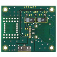
Page 18
... An 9.998 example layout is shown in Figure 45 and Figure 46. 19.93 50.40 100.0 199.4 495.0 991 Rev Page Figure 45. Top Layer of the AD8221-EVAL Figure 46. Bottom Layer of the AD8221-EVAL ...
Page 19
... S Figure 47. Supply Decoupling, REF, and Output Referred to Local Ground INPUT BIAS CURRENT RETURN PATH The input bias current of the AD8221 must have a return path to common. When the source, such as a thermocouple, cannot provide a return current path, one should be created, as shown in Figure 48. ...
Page 20
... By using a value the mismatch is reduced, and therefore, performance is improved. PRECISION STRAIN GAGE The low offset and high CMRR over frequency of the AD8221 make it an excellent candidate for bridge measurements. As shown in Figure 50, the bridge can be directly connected to the inputs of the amplifier. 350Ω ...
Page 21
... The fourth benefit of this interface circuit is that the acquisition time of the AD8221 is reduced by a factor of 2. With the help of the OP27, the AD8221 only needs to deliver one-half of the full swing; therefore, signals can settle more quickly. Lastly, the AD8022 settles quickly, which is helpful because the shorter the settling time, the more bits that can be resolved when the ADC acquires data ...
Page 22
... AD8221 DIE INFORMATION Die size: 1575 μm × 2230 μm Die thickness: 381 μm To minimize gain errors introduced by the bond wires, use Kelvin connections between the chip and the gain resistor, R Pad 2A and Pad 2B in parallel to one end of R where R is not required, Pad 2A and Pad 2B must be bonded together as well as the Pad 3A and Pad 3B. ...
Page 23
... PARENTHESES) ARE ROUNDED-OFF MILLIMETER EQUIVALENTS FOR REFERENCE ONLY AND ARE NOT APPROPRIATE FOR USE IN DESIGN. Figure 55. 8-Lead Standard Small Outline Package [SOIC_N] Narrow Body (R-8) Dimensions shown in millimeters and (inches) Rev Page 0.80 0.55 0.40 0.50 (0.0196) 45° 0.25 (0.0099) 1.27 (0.0500) 0.40 (0.0157) AD8221 ...
Page 24
... AD8221ARZ-R7 –40°C to +85°C AD8221ARZ-RL –40°C to +85°C AD8221ARM –40°C to +85°C AD8221ARM-REEL –40°C to +85°C AD8221ARM REEL7 –40°C to +85°C AD8221ARMZ –40°C to +85°C AD8221ARMZ-R7 –40°C to +85°C AD8221ARMZ-RL –40°C to +85°C AD8221BR – ...