AD8225-EVAL Analog Devices Inc, AD8225-EVAL Datasheet - Page 3
AD8225-EVAL
Manufacturer Part Number
AD8225-EVAL
Description
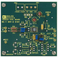
BOARD EVAL FOR AD8225
Manufacturer
Analog Devices Inc
Specifications of AD8225-EVAL
Lead Free Status / RoHS Status
Contains lead / RoHS non-compliant


SPECIFICATIONS
Parameter
GAIN
VOLTAGE OFFSET (RTI)
INPUT
OUTPUT
DYNAMIC RESPONSE
NOISE (RTI)
REFERENCE INPUT
POWER SUPPLY
TEMPERATURE RANGE
*Pin 1 connected to Pin 4. See Applications section.
Specifications subject to change without notice.
REV. A
Gain
Gain Error
Nonlinearity
vs. Temperature
Offset Voltage
vs. Temperature
vs. Supply
Input Operating Impedance
Input Operating Voltage Range
Input Bias Current
Input Offset Current
Common-Mode Rejection Ratio
Operating Voltage Range
Operating Voltage Range
Short Circuit Current
Small Signal –3 dB Bandwidth
Full Power Bandwidth
Settling Time (0.01%)
Settling Time (0.001%)
Slew Rate
Voltage
Current
R
I
Voltage Range
Gain to Output
Operating Range
Quiescent Current
For Specified Performance
IN
IN
Differential
Common-Mode
vs. Temperature
vs. Temperature
vs. Temperature
vs. Temperature
vs. Temperature
(T
A
= 25 C, V
Conditions
T
f = 10 kHz*
R
R
V
7 V Step
7 V Step
0.1 Hz to 10 Hz
Spectral Density, 1 kHz
0.1 Hz to 10 Hz
Spectral Density, 1 kHz
V
A
L
L
OUT
INT
= 2 kΩ
= 10 kΩ
= T
, V
= 7.8 V p-p
S
MIN
REF
=
to T
= 0
5 V, R
MAX
L
= 2 k , unless otherwise noted.)
–3–
Min
–0.1
90
–V
–V
86
83
80
–V
–V
–V
–V
5
–V
1.7
–40
0.999
S
S
S
S
S
S
S
+ 1.6
+ 2.1
+ 0.9
+ 1.0
+ 0.8
+ 0.9
+ 0.9
10 2
Typ
5
+0.05
2
1
125
100
10 2
0.5
3
0.15
1.5
94
18
900
170
3
4.3
1.5
45
4
50
18
60
1
1.05
Max
+0.1
10
5
325
2
+V
+V
1.2
0.5
+V
+V
+V
+V
+V
1.001
18
1.2
+85
S
S
S
S
S
S
S
– 1.0
– 1.5
– 1.0
– 1.2
– 1.0
– 1.0
– 1.0
Unit
V/V
%
± ppm
± ppm/°C
±µV
±µV/°C
dB
GΩ pF
GΩ pF
V
V
nA
pA/°C
nA
pA/°C
dB
dB
dB
V
V
V
V
mA
kHz
kHz
µs
µs
V/µs
µV p-p
nV/√Hz
pA p-p
fA/√Hz
kΩ
µA
V
± V
mA
°C
AD8225
Related parts for AD8225-EVAL
Image
Part Number
Description
Manufacturer
Datasheet
Request
R

Part Number:
Description:
BOARD EVAL FOR AD8225 INSTR AMP
Manufacturer:
Analog Devices Inc
Datasheet:

Part Number:
Description:
±1.7g Dual-Axis IMEMS Accelerometer Evaluation Board
Manufacturer:
Analog Devices Inc
Datasheet:
Part Number:
Description:
Inertial Sensor Evaluation System
Manufacturer:
Analog Devices Inc
Datasheet:
Part Number:
Description:
Manufacturer:
Analog Devices Inc
Datasheet:
Part Number:
Description:
Manufacturer:
Analog Devices Inc
Datasheet:
Part Number:
Description:
Manufacturer:
Analog Devices Inc
Datasheet:
Part Number:
Description:
Manufacturer:
Analog Devices Inc
Datasheet:
Part Number:
Description:
Manufacturer:
Analog Devices Inc
Datasheet:
Part Number:
Description:
Manufacturer:
Analog Devices Inc
Datasheet:
Part Number:
Description:
Manufacturer:
Analog Devices Inc
Datasheet:
Part Number:
Description:
Manufacturer:
Analog Devices Inc
Datasheet:
Part Number:
Description:
Manufacturer:
Analog Devices Inc
Datasheet:
Part Number:
Description:
Manufacturer:
Analog Devices Inc
Datasheet: