AD629-EVAL Analog Devices Inc, AD629-EVAL Datasheet
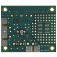
AD629-EVAL
Specifications of AD629-EVAL


Related parts for AD629-EVAL


AD629-EVAL Summary of contents
Page 1
... V common-mode voltage range and has inputs that are protected from common-mode or differential mode transients up to ±500 V. The AD629 has low offset, low offset drift, low gain error drift, low common-mode rejection drift, and excellent CMRR over a wide frequency range. ...
Page 2
... AD629 TABLE OF CONTENTS Features .............................................................................................. 1 Applications....................................................................................... 1 Functional Block Diagram .............................................................. 1 General Description ......................................................................... 1 Revision History ............................................................................... 2 Specifications..................................................................................... 3 Absolute Maximum Ratings............................................................ 4 ESD Caution.................................................................................. 4 Typical Performance Characteristics ............................................. 5 Theory of Operation ........................................................................ 9 Applications..................................................................................... 10 REVISION HISTORY 3/07—Rev Rev. B Updated Format and Layout .............................................Universal Changes to Ordering Guide .......................................................... 15 3/00—Rev Rev. A 10/99—Revision 0: Initial Version Basic Connections ...
Page 3
... AD629 Unit V/V % ppm ppm ppm/° μV/° kΩ kΩ kHz V/μs kHz μs μs μs μV p-p nV/√ °C ...
Page 4
... AD629 ABSOLUTE MAXIMUM RATINGS Table 2. Parameter Supply Voltage Internal Power Dissipation 8-Lead PDIP (N) 8-Lead SOIC (R) Input Voltage Range, Continuous Common-Mode and Differential, 10 sec Output Short-Circuit Duration Pin 1 and Pin 5 Maximum Junction Temperature Operating Temperature Range Storage Temperature Range Lead Temperature (Soldering 60 sec) ...
Page 5
... OUT = 2 kΩ (Curves Offset for Clarity ±5V 10kΩ ±5V 2kΩ ±5V 1kΩ ±2.5V 1kΩ –20 –16 –12 –8 – (V) OUT = 0 V and Output Voltage OUT Operating Range vs. Supply Voltage (Curves Offset for Clarity) AD629 T = –40° 2kΩ L 4V/DIV 1V/DIV ...
Page 6
... AD629 20µV/DIV –10 – (V) OUT Figure 11. Gain Nonlinearity ± 20µV/DIV –10 –8 –6 –4 – (V) OUT Figure 12. Gain Nonlinearity ± 40µV/DIV –3.0 –2.4 –1.8 –1.2 –0.6 0 0.6 V (V) OUT Figure 13. Gain Nonlinearity ± ±15V 10kΩ L 2.5V/DIV kΩ ±12V 10kΩ ...
Page 7
... Figure 19. Voltage Noise Spectral Density vs. Frequency –40°C +25°C +85°C +25° ± 10k 1k 10k 100k Rev Page 2kΩ 1000pF L 25mV/DIV 4µs/DIV Figure 20. Small Signal Pulse Response 2kΩ 1000pF L 25mV/DIV 4µs/DIV Figure 21. Small Signal Pulse Response 2kΩ 1000pF L 5V/DIV 5µs/DIV Figure 22. Large Signal Pulse Response AD629 ...
Page 8
... AD629 5V/DIV +10V V OUT 0V OUTPUT ERROR 1mV/DIV Figure 23. Settling Time to 0.01%, for Output Step −1, R 350 N = 2180 300 n ≈ 200 PCS. FROM 10 ASSEMBLY LOTS 250 200 150 100 50 0 –150 –100 –50 0 COMMON-MODE REJECTION RATIO (ppm) Figure 24. Typical Distribution of Common-Mode Rejection; Package Option N-8 ...
Page 9
... THEORY OF OPERATION The AD629 is a unity gain, differential-to-single-ended amplifier (diff amp) that can reject extremely high common- mode signals (in excess of 270 V with 15 V supplies). It consists of an operational amplifier (op amp) and a resistor network. To achieve high common-mode voltage range, an internal resistor divider (Pin 3 or Pin 5) attenuates the noninverting signal by a factor of 20 ...
Page 10
... Failure to do this results in degraded common- mode rejection. Pin connect pin and should be left open. SINGLE-SUPPLY OPERATION Figure 31 shows the connections for operating the AD629 with a single supply. Because the output can swing to within only about either rail necessary to apply an offset to the output. This can be conveniently done by connecting REF(+) and REF(– ...
Page 11
... V dc with shunt resistors from GND +5V 20 Ω to 2000 Ω. Assuming that the shunt resistor is selected to use the full ±10 V output swing of the AD629, the error voltage becomes quite significant as R 0.1µF 14 Table 3. Error Resulting from Large Values of R ...
Page 12
... AD629 OUTPUT CURRENT AND BUFFERING The AD629 is designed to drive loads of 2 kΩ to within the rails but can deliver higher output currents at lower output voltages (see Figure 15). If higher output current is required, the output of the AD629 should be buffered with a precision op amp, such as the OP113, as shown in Figure 36. This op amp can swing to within either rail while driving a load as small as 600 Ω ...
Page 13
... Note that the same kind of power-line interference can happen as detailed in Example 1. However, the ac common-mode component of 200 V p-p coming from the shunt is much larger than the interference p-p; therefore, this interference component can be neglected. Table 6. AD629 vs. INA117 AC Error Budget Example 2 (V Error Source ACCURACY 25°C A ...
Page 14
... AD629 OUTLINE DIMENSIONS 0.210 (5.33) MAX 0.150 (3.81) 0.130 (3.30) 0.115 (2.92) 0.022 (0.56) 0.018 (0.46) 0.014 (0.36) CONTROLLING DIMENSIONS ARE IN INCHES; MILLIMETER DIMENSIONS (IN PARENTHESES) ARE ROUNDED-OFF INCH EQUIVALENTS FOR REFERENCE ONLY AND ARE NOT APPROPRIATE FOR USE IN DESIGN. CORNER LEADS MAY BE CONFIGURED AS WHOLE OR HALF LEADS. ...
Page 15
... AD629BRZ –40°C to +85°C 1 AD629BRZ-RL –40°C to +85°C 1 AD629BRZ-R7 –40°C to +85°C AD629-EVAL RoHS compliant part. Package Description 8-Lead PDIP 8-Lead PDIP 8-Lead SOIC_N 8-Lead SOIC_N 8-Lead SOIC_N 8-Lead SOIC_N 8-Lead SOIC_N, 13-Inch Tape and Reel, 2,500 pieces ...
Page 16
... AD629 NOTES ©1999-2007 Analog Devices, Inc. All rights reserved. Trademarks and registered trademarks are the property of their respective owners. D00783-0-2/07(B) Rev Page ...