ATSTK501 Atmel, ATSTK501 Datasheet - Page 14
ATSTK501
Manufacturer Part Number
ATSTK501
Description
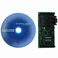
ADAPTER KIT FOR 64PIN AVR MCU
Manufacturer
Atmel
Datasheet
1.ATSTK501.pdf
(29 pages)
Specifications of ATSTK501
Accessory Type
STK500 Expansion Module
Processor To Be Evaluated
ATmega103 and ATmega128
Data Bus Width
8 bit
Interface Type
RS-232
For Use With/related Products
64-pin megaAVR Devices
For Use With
ATADAPCAN01 - EXTENSION CAN ADD-ON TO STK500/1ATSTK500 - PROGRAMMER AVR STARTER KIT
Lead Free Status / RoHS Status
Lead free / RoHS Compliant
Other names
Q1167170
STK501
STK501
STK501
STK501


Using the STK501 Top Module
2.6
2.7
2.8
2-8
Ram High
Address
Jumpers
A[7:0] Connector
Using the SRAM
Interface with
AT90S/LS8515
and ATmega161
Figure 2-11. SRAMEN Connected to GND
When External Memory is enabled in an AVR, all Port C pins are by default used for the
high address byte. If the full 60 KB address space is not required to access the external
memory, some, or all, Port C pins can be released for normal port pin function as
described in the ATmega128(L) datasheet. AT90S/LS8515, ATmega103(L) and
ATmega161 do not have this feature, and all jumpers should be connected if using the
XRAM interface with these devices.
If some or all of the Port C pins are released for normal port pin functions, the corre-
sponding “RAM High Address” jumper should be removed to avoid any Port C activity to
reach the SRAM address pins thus corrupting the address.
If a jumper is removed, the corresponding address line will be pulled low giving a logic
zero on that address bit on the SRAM. See the block schematic on Figure 2-10.
The connector marked A[7:0] contains the 8 least-significant bits of the external SRAM
address bus. The purpose of the connector is to provide easy access to the address
bus. The 8 most significant bits can be found on the “Ram High Addresses” jumpers or
the Port C connector.
The connector is placed after the latch as shown in Figure 2-10.
This connector is handy when using the SRAM interface to interface external devices.
When using the SRAM interface with devices placed in the STK500 board, some addi-
tional straps are required. The reason is that the RD, WR, and ALE signals are not on
the same port pins for the AT90S8515/ATmega161(L) and ATmega103(L)/
ATmega128(L), so these signals must be routed manually using two of the 2-wire
cables.
Table 2-2. Signal Routing Required for AT90S8515A and ATmega161(L)
Connections
Write Signal WR
Read Signal RD
Address Latch Enable ALE
STK500
PD6
PD7
PE1
STK501
PG0
PG1
PG2
Description
Connect PD6:STK500 to PG0:STK501
Connect PD7:STK500 to PG1:STK501
Connect PE1:STK500 to PG2:STK501
AVR
®
STK501 User Guide
Related parts for ATSTK501
Image
Part Number
Description
Manufacturer
Datasheet
Request
R

Part Number:
Description:
DEV KIT FOR AVR/AVR32
Manufacturer:
Atmel
Datasheet:

Part Number:
Description:
INTERVAL AND WIPE/WASH WIPER CONTROL IC WITH DELAY
Manufacturer:
ATMEL Corporation
Datasheet:
Part Number:
Description:
Low-Voltage Voice-Switched IC for Hands-Free Operation
Manufacturer:
ATMEL Corporation
Datasheet:
Part Number:
Description:
MONOLITHIC INTEGRATED FEATUREPHONE CIRCUIT
Manufacturer:
ATMEL Corporation
Datasheet:
Part Number:
Description:
AM-FM Receiver IC U4255BM-M
Manufacturer:
ATMEL Corporation
Datasheet:
Part Number:
Description:
Monolithic Integrated Feature Phone Circuit
Manufacturer:
ATMEL Corporation
Datasheet:
Part Number:
Description:
Multistandard Video-IF and Quasi Parallel Sound Processing
Manufacturer:
ATMEL Corporation
Datasheet:
Part Number:
Description:
High-performance EE PLD
Manufacturer:
ATMEL Corporation
Datasheet:
Part Number:
Description:
8-bit Flash Microcontroller
Manufacturer:
ATMEL Corporation
Datasheet:
Part Number:
Description:
2-Wire Serial EEPROM
Manufacturer:
ATMEL Corporation
Datasheet: