NBSG111BAEVB ON Semiconductor, NBSG111BAEVB Datasheet - Page 2
NBSG111BAEVB
Manufacturer Part Number
NBSG111BAEVB
Description
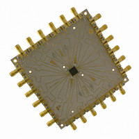
BOARD EVALUATION BBG NBSG111BA
Manufacturer
ON Semiconductor
Specifications of NBSG111BAEVB
Main Purpose
Clock/Data Driver
Utilized Ic / Part
NBSG111
Primary Attributes
W/RSECL Outputs
Technology Type
Evaluation Board
Lead Free Status / RoHS Status
Contains lead / RoHS non-compliant
For Use With/related Products
NBSG111
Other names
NBSG111BAEVB
NBSG111BAEVBOS
NBSG111BAEVBOS


Setup
NOTE:
Step 1:
Step 2:
Amplitude = 500 mV
Offset = 660 mV
Signal Generator
Table 1. Basic Equipment
1. Equipment used to generate example measurements within this document.
2. 50 GHz sample module used (for effective rise, fall and jitter performance measurement)
All differential cable pairs must be matched.
Due to simplifcation of the block diagram CLK1/CLK1 and Q1 − Q8 connections are not shown.
Power Supply with 2 outputs
Oscilloscope
Differential Signal Generator
Matched high speed cables with SMA connectors
Power Supply cables with clips
TRIGGER
NOTE:
Connect Power
Connect Inputs
For Differential Mode (3.3 V and 2.5 V operation)
For Single−Ended Mode (3.3 V operation only)
1a: Three power levels must be provided to the board for V
face mount clips. Using the split power supply mode, GND = V
2a: Connect the differential output of the generator to the differential input of the device
(CLK0 and CLK0).
2a: Connect the AC coupled single−ended output generator to input.
OUT
OUT
For best results, unconnected input should be terminated to V
V
V
EE
EE
Description
= −1.3 V (3.3 V op)
= −0.5 V (2.5 V op)
−or−
Figure 2. NBSG111 Board Setup − Time Domain
V
3.3 V Setup
Setup for Time Domain Measurements
V
V
EE
CC
TT
V
CLK0
CLK0
V
V
CC
= −1.3 V
CC
EE
= 2.0 V
= GND
= 2.0 V
Power Supply Connections
SEL
NBSG111BAEVB
(Differential Mode)
EN
http://onsemi.com
V
V
CC
CC
SEL
EN
HP6624A
TDS8000 with 80E01 Sampling Head (Note 2)
HP 8133A, Advantest D3186
Storm, Semflex
2
Float
Float
V
V
TT
TT
GND
GND
= 0 V
Example Equipment (Note 1)
= 0 V
V
2.5 V Setup
V
V
Q0
Q0
Q9
EE
Q9
CC
TT
CC
= −0.5 V
= 2.0 V
= GND
TT
, V
through 50 W resistor
TT
EE
, and GND via the sur-
= V
CC
– 2.0 V.
Channel 1
Channel 2
Channel 3
Channel 4
Channel 5
Channel 6
Channel 7
Channel 8
TRIGGER
* Q0 − Q9 Ouputs
Digital Oscilloscope
Qty.
10
1
1
1
3
Related parts for NBSG111BAEVB
Image
Part Number
Description
Manufacturer
Datasheet
Request
R

Part Number:
Description:
2.5v/3.3v Sige Differential 1 10 Clock/data Driver With Rsecl Outputs
Manufacturer:
ON Semiconductor
Datasheet:
Part Number:
Description:
ON Semiconductor [VOLTAGE REGULATOR]
Manufacturer:
ON Semiconductor
Datasheet:
Part Number:
Description:
357-036-542-201 CARDEDGE 36POS DL .156 BLK LOPRO
Manufacturer:
ON Semiconductor
Datasheet:
Part Number:
Description:
357-036-542-201 CARDEDGE 36POS DL .156 BLK LOPRO
Manufacturer:
ON Semiconductor
Datasheet:
Part Number:
Description:
357-036-542-201 CARDEDGE 36POS DL .156 BLK LOPRO
Manufacturer:
ON Semiconductor
Datasheet:
Part Number:
Description:
357-036-542-201 CARDEDGE 36POS DL .156 BLK LOPRO
Manufacturer:
ON Semiconductor
Datasheet:
Part Number:
Description:
357-036-542-201 CARDEDGE 36POS DL .156 BLK LOPRO
Manufacturer:
ON Semiconductor
Datasheet:
Part Number:
Description:
357-036-542-201 CARDEDGE 36POS DL .156 BLK LOPRO
Manufacturer:
ON Semiconductor
Datasheet:
Part Number:
Description:
357-036-542-201 CARDEDGE 36POS DL .156 BLK LOPRO
Manufacturer:
ON Semiconductor
Datasheet:
Part Number:
Description:
357-036-542-201 CARDEDGE 36POS DL .156 BLK LOPRO
Manufacturer:
ON Semiconductor
Datasheet:
Part Number:
Description:
357-036-542-201 CARDEDGE 36POS DL .156 BLK LOPRO
Manufacturer:
ON Semiconductor
Datasheet:
Part Number:
Description:
357-036-542-201 CARDEDGE 36POS DL .156 BLK LOPRO
Manufacturer:
ON Semiconductor
Datasheet:
Part Number:
Description:
Manufacturer:
ON Semiconductor
Datasheet:
Part Number:
Description:
Manufacturer:
ON Semiconductor
Datasheet: