MPC8349E-MITXE Freescale Semiconductor, MPC8349E-MITXE Datasheet - Page 12
MPC8349E-MITXE
Manufacturer Part Number
MPC8349E-MITXE
Description
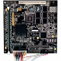
BOARD REFERENCE FOR MPC8349
Manufacturer
Freescale Semiconductor
Series
PowerQUICC II™ PROr
Type
MPUr
Specifications of MPC8349E-MITXE
Contents
Module and Misc Hardware
Processor To Be Evaluated
MPC8349E
Interface Type
Ethernet, USB
Silicon Manufacturer
Freescale
Core Architecture
Power Architecture
Core Sub-architecture
PowerQUICC
Silicon Core Number
MPC83xx
Silicon Family Name
PowerQUICC II PRO
Rohs Compliant
Yes
For Use With/related Products
MPC8349E
Lead Free Status / RoHS Status
Lead free / RoHS Compliant
Other names
MPC8349E-MITXE


MPC8349E-mITXE Board
The DS1339 RTC is connected to I
or write to the RTC through the I2C2 interface.
1.2.8
A compact Flash interface connects directly to the local bus without a PCMCIA controller. The true IDE
mode is the only compact Flash operating mode supported by this connection. Hot insertion and removal
is not supported. The MPC8349E universal programmable machine A (UPMA) is used to generate the
required timing for IORD and IOWR through the LGPL0 and LGPL1 signals.
The true IDE mode requires three address signals (A[0:2]) and two chip-enable signals (CE[1:2]) to
address the 10 registers in the AT task file. Therefore, glue logic is used to split CS3 into two regions. One
chip-select signal (CS3) is assigned to the compact Flash interface. Glue logic is used to generate the CE1
and CE2 signals required by the compact Flash. The logic simply uses the local bus address A22 to
determine which chip-enable signal is generated. See
12
(U10) bit[0..7]
PCF8574A
4
5
6
7
Compact Flash Interface
MPCI_CLKRUN
PCI_M66EN
Not used
BOOT0
Name
MPC8349E-mITXE Reference Design Platform User’s Guide, Rev. 2
LBA22
Table 5. PCF8574A (U10) Bit Descriptions (continued)
CS3
Figure 7. CE1 and CE2 Generation Logic
Read only, write
Read only, write
Preliminary—Subject to Change Without Notice
has no effect
has no effect
2
Read/Write
Read/Write
C with address 0x68. The software running on PowerPC core can read
—
MiniPCI clock run signal level, defined by the PCI Mobile Design
Guide.
0: MiniPCI clock is in normal operating frequency
1: MiniPCI clock is stopped or running very low
PCI M66EN Signal
0: PCI M66EN signal is low, indicates the PCI cards on PCI slot and
1: PCI M66EN signal is high, indicates the PCI cards on PCI slot and
Used to determine which Flash is used for boot Flash
0: Flash 0 (U4) is the boot Flash
1: Flash 1 (U7) is the boot Flash
—
miniPCI slot are not 66 MHz capable
miniPCI slot are 66 MHz capable
Figure
7.
Description
CE2
CE1
Freescale Semiconductor
Related parts for MPC8349E-MITXE
Image
Part Number
Description
Manufacturer
Datasheet
Request
R

Part Number:
Description:
KIT REFERENCE PLATFORM MPC8349E
Manufacturer:
Freescale Semiconductor
Datasheet:
Part Number:
Description:
KIT MODULAR DEV SYSTEM MPC8349E
Manufacturer:
Freescale Semiconductor
Datasheet:

Part Number:
Description:
MCU, MPU & DSP Development Tools PROCESSR BD MPC8349E
Manufacturer:
Freescale Semiconductor
Part Number:
Description:
MCU, MPU & DSP Development Tools KIT FOR MPC8349E BDS
Manufacturer:
Freescale Semiconductor

Part Number:
Description:
Manufacturer:
Freescale Semiconductor, Inc
Datasheet:
Part Number:
Description:
Manufacturer:
Freescale Semiconductor, Inc
Datasheet:
Part Number:
Description:
Manufacturer:
Freescale Semiconductor, Inc
Datasheet:
Part Number:
Description:
Manufacturer:
Freescale Semiconductor, Inc
Datasheet:
Part Number:
Description:
Manufacturer:
Freescale Semiconductor, Inc
Datasheet:
Part Number:
Description:
Manufacturer:
Freescale Semiconductor, Inc
Datasheet:
Part Number:
Description:
Manufacturer:
Freescale Semiconductor, Inc
Datasheet:
Part Number:
Description:
Manufacturer:
Freescale Semiconductor, Inc
Datasheet:
Part Number:
Description:
Manufacturer:
Freescale Semiconductor, Inc
Datasheet:
Part Number:
Description:
Manufacturer:
Freescale Semiconductor, Inc
Datasheet:
Part Number:
Description:
Manufacturer:
Freescale Semiconductor, Inc
Datasheet: