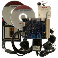
C8051F930DK Silicon Laboratories Inc, C8051F930DK Datasheet - Page 23

C8051F930DK
Manufacturer Part Number
C8051F930DK
Description
KIT DEV C8051F920,F921,F930,F931
Manufacturer
Silicon Laboratories Inc
Type
MCUr
Specifications of C8051F930DK
Contents
Target Board, Power Adapter, USB Debug Adapter, Cables, Batteries, and Software
Processor To Be Evaluated
C8051F930
Processor Series
C8051F9xx
Data Bus Width
8 bit
Interface Type
I2C, UART, SPI
Maximum Operating Temperature
+ 85 C
Minimum Operating Temperature
- 40 C
Operating Supply Voltage
0.9 V to 3.6 V
Lead Free Status / RoHS Status
Lead free / RoHS Compliant
For Use With/related Products
C8051F920, F921, F930, F931
Lead Free Status / Rohs Status
Lead free / RoHS Compliant
Other names
336-1473
Available stocks
Company
Part Number
Manufacturer
Quantity
Price
Company:
Part Number:
C8051F930DK
Manufacturer:
Silicon Labs
Quantity:
135
11. When the missing clock detector is enabled, why does the MCU reset if I switch from the default system
12.Why is the MCU pre-maturely released from reset when using a wall supply with a slow rise time?
clock (Low Power Oscillator divided by 8) to smaRTClock divided by 1?
Background:
—The missing clock detector will trigger a reset if the system clock period exceeds 100 µs.
—Switchover between clock sources occurs in 1 clock cycle of the slowest clock.
—Changing the clock divide value requires up to 128 cycles of the undivided clock source.
Since the clock source change occurs in a single cycle and the clock divide change can take up to 128
cycles, the system clock will be set to the new clock source divided by the old divide value for a brief period
of time. In this example, the actual system clock will be 4.096 kHz for up to 128 cycles of the undivided clock
source. This causes the missing clock detector to time out and reset the MCU.
The proper way of changing the system clock when both the clock source and the clock divide value are
being changed is as follows:
If switching from a fast “undivided” clock to a slower “undivided” clock:
If switching from a fast “undivided” clock to a slower “undivided” clock:
The maximum VDD Ramp Time is specified at 3 ms. If the power supply ramp takes longer than 3 ms to reach
0.9 V, then the device may be released from reset before the supply has reached the minimum operating
voltage. The slow ramp time (>3 ms) can occur when using a bench power supply that does not have an output
enable switch.
a. Change the clock divide value.
b. Poll for CLKRDY > 1.
c. Change the clock source.
d. Change the clock source.
e. Change the clock divide value.
f.
Poll for CLKRDY > 1.
Rev. 0.5
C8051F930-DK
23


