C8051F064EK Silicon Laboratories Inc, C8051F064EK Datasheet - Page 12
C8051F064EK
Manufacturer Part Number
C8051F064EK
Description
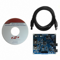
KIT EVAL FOR C8051F064
Manufacturer
Silicon Laboratories Inc
Type
MCUr
Specifications of C8051F064EK
Contents
Evaluation Board, Power Supply, USB Cables, Adapter and Documentation
Processor To Be Evaluated
C8051F06x
Interface Type
USB
Silicon Manufacturer
Silicon Labs
Core Architecture
8051
Silicon Core Number
C8051F064
Silicon Family Name
C8051F06x
Lead Free Status / RoHS Status
Contains lead / RoHS non-compliant
For Use With/related Products
C8051F064
Lead Free Status / Rohs Status
Lead free / RoHS Compliant
Other names
336-1219


C8051F064-EK
9.7. External Memory Interface (J11, J14)
The C8051F064 evaluation board provides an External Memory Interface by connecting a 128 kB SRAM to the
device port pins. The device’s External Memory Interface can be enabled by installing a shorting block at header
J11. This connects port pin P4.5 to the Chip Select (CS) signal on the SRAM, pulling this signal low. Placing a
shorting block on header J14, Pin 2 and Pin 3, enables the use of the lower address bank on the SRAM. Moving
the shorting block to J14, Pin 1 and Pin 2, enables port pin P3.7 to select between the upper and lower address
banks on the SRAM. Refer to Table 4 for the external memory interface signal descriptions.
9.8. PORT I/O Connectors (J15)
The Port 0 signals on the C8051F064 have their own 10-pin header (J15). This header provides a pin for each of
the corresponding port pins 0-7, +3.3 V and digital ground. See Table 5 for the J15 pin connections.
12
Table 4. External Memory Interface Signal Descriptions
SRAM Signal
I/O0...I/O7
A8...A15
A0...A7
Table 5. J15 Port Connector Pin Descriptions
GND
V
A16
A16
WE
CS
OE
DD
Pin #
10
1
2
3
4
5
6
7
8
9
C8051F060 Signal
GND (J14[2-3])
P3.7 (J14[1-2])
P7.0...P7.7
P6.0...P6.7
P5.0...P5.7
P4.5 (J11)
+3VD2
GND
P4.7
P4.6
Rev. 0.4
+3 VD (+3.3 V)
GND (Ground)
Description
P0.0
P0.1
P0.2
P0.3
P0.4
P0.5
P0.6
P0.7
Address Bus High Byte
Address Bus Low Byte
Bank Select Always 0
Output Enable
Digital Ground
Digital Power
Write Enable
Description
Bank Select
Chip Select
Data Bus
Related parts for C8051F064EK
Image
Part Number
Description
Manufacturer
Datasheet
Request
R

Part Number:
Description:
SMD/C°/SINGLE-ENDED OUTPUT SILICON OSCILLATOR
Manufacturer:
Silicon Laboratories Inc
Part Number:
Description:
Manufacturer:
Silicon Laboratories Inc
Datasheet:
Part Number:
Description:
N/A N/A/SI4010 AES KEYFOB DEMO WITH LCD RX
Manufacturer:
Silicon Laboratories Inc
Datasheet:
Part Number:
Description:
N/A N/A/SI4010 SIMPLIFIED KEY FOB DEMO WITH LED RX
Manufacturer:
Silicon Laboratories Inc
Datasheet:
Part Number:
Description:
N/A/-40 TO 85 OC/EZLINK MODULE; F930/4432 HIGH BAND (REV E/B1)
Manufacturer:
Silicon Laboratories Inc
Part Number:
Description:
EZLink Module; F930/4432 Low Band (rev e/B1)
Manufacturer:
Silicon Laboratories Inc
Part Number:
Description:
I°/4460 10 DBM RADIO TEST CARD 434 MHZ
Manufacturer:
Silicon Laboratories Inc
Part Number:
Description:
I°/4461 14 DBM RADIO TEST CARD 868 MHZ
Manufacturer:
Silicon Laboratories Inc
Part Number:
Description:
I°/4463 20 DBM RFSWITCH RADIO TEST CARD 460 MHZ
Manufacturer:
Silicon Laboratories Inc
Part Number:
Description:
I°/4463 20 DBM RADIO TEST CARD 868 MHZ
Manufacturer:
Silicon Laboratories Inc
Part Number:
Description:
I°/4463 27 DBM RADIO TEST CARD 868 MHZ
Manufacturer:
Silicon Laboratories Inc
Part Number:
Description:
I°/4463 SKYWORKS 30 DBM RADIO TEST CARD 915 MHZ
Manufacturer:
Silicon Laboratories Inc
Part Number:
Description:
N/A N/A/-40 TO 85 OC/4463 RFMD 30 DBM RADIO TEST CARD 915 MHZ
Manufacturer:
Silicon Laboratories Inc
Part Number:
Description:
I°/4463 20 DBM RADIO TEST CARD 169 MHZ
Manufacturer:
Silicon Laboratories Inc