C8051F996-TB Silicon Laboratories Inc, C8051F996-TB Datasheet
C8051F996-TB
Specifications of C8051F996-TB
Available stocks


Related parts for C8051F996-TB

C8051F996-TB Summary of contents
Page 1
... The target board included in this kit is provided with a pre-soldered C8051F996 MCU (QSOP24 package). Code developed on the C8051F996 can be easily ported to the other members of this MCU family. Refer to the C8051F99x-C8051F98x data sheet for the differences between the members of this MCU family. ...
Page 2
... C8051F996-DK 3. Hardware Setup Refer to Figure 2 for a diagram of the hardware configuration. 1. Connect the USB Debug Adapter to the DEBUG connector on the target board with the 10-pin ribbon cable. 2. Connect one end of the USB cable to the USB connector on the USB Debug Adapter. 3. Verify that a shorting block is installed on J17 and that SW5 is in the ON position. ...
Page 3
... To install the IDE, utilities, and code examples, perform the following steps: 1. Click on the "Install Development Tools" button on the installation utility's startup screen the Kit Selection box that appears, choose the C8051F996-DK development kit from the list of options the next screen, choose “Components to be Installed”. The programs necessary to download and debug on the MCU are the Silicon Labs IDE and the 8051 Evaluation Toolset ...
Page 4
... C8051F996-DK 5. Software Overview The following software is necessary to build a project, download code to, and communicate with the target microcontroller. 8051 Evaluation Toolset Silicon Labs Integrated Development Environment (IDE) Other useful software that is provided on the development kit CD and the Silicon Labs Downloads (www.silabs.com/mcudownloads) website includes: ...
Page 5
... Save the project when finished with the debug session to preserve the current target build configuration, editor settings and the location of all open debug views. To save the project, select Project As... from the menu. Create a new name for the project and click on Save. C8051F996-DK Target Build Configuration dialog. If errors occur during the ...
Page 6
... C8051F996-DK 5.3. Configuration Wizard 2 The Configuration Wizard code generation tool for all of the Silicon Labs devices. Code is generated through the use of dialog boxes for each of the device's peripherals. Figure 3. Configuration Wizard 2 Utility The Configuration Wizard 2 utility helps accelerate development by automatically generating initialization source code to configure and enable the on-chip resources needed by most design projects ...
Page 7
... To create a new profile: 1. Select the profile that most closely matches the target application or choose the "Custom Profile". 2. Click Manage 3. Click Duplicate 4. Click Edit Profiles may be edited with the easy-to-use GUI (shown in Figure 5). C8051F996-DK Rev. 0.1 7 ...
Page 8
... C8051F996-DK Figure 5. Battery Life Estimator Discharge Profile Editor The Discharge Profile Editor allows the user to modify the profile name and description. The four text entry boxes on the left hand side of the form allow the user to specify the amount of time the system spends in each power mode ...
Page 9
... The primary outputs of the Battery Life Estimator are an estimated system operating time and a simulated graph of battery voltage vs. time. Additional outputs include estimated battery capacity, average current, self-discharge current, and the ability to export graph data to a comma delimited text file for plotting in an external graphing application. C8051F996-DK Rev. 0.1 9 ...
Page 10
... Port I/O crossbar, configuring a timer for an interrupt routine, initializing the system clock, and configuring a GPIO port pin. When compiled/assembled and linked this program flashes the LED on the C8051F996 Target Board about five times a second using the interrupt handler with a C8051F996 timer. ...
Page 11
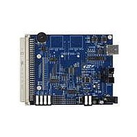
... Target Board The C8051F996 Development Kit includes a target board with a C8051F996 device pre-installed for evaluation and preliminary software development. Numerous input/output (I/O) connections are provided to facilitate prototyping using the target board. Refer to Figure 7 for the locations of the various I/O connectors. Figure 9 on page 13 shows the factory default shorting block positions ...
Page 12
... The following items are located on the bottom side of the board. See Figure 8. BH1 Battery Holder for 1.5 V AAA. BH2 Battery Holder for 1.5 V AAA. BH3 Battery Holder for 3 V Coin Cell (CR2032). BH2 (AAA) Figure 8. Bottom of C8051F996 Target Board 12 NEG POS BH3 (CR2032) POS NEG Rev. 0.1 ...
Page 13
... Target Board Shorting Blocks: Factory Defaults The C8051F996 Target Board comes from the factory with pre-installed shorting blocks on many headers. Figure 9 shows the positions of the factory default shorting blocks. R15 J16 P1.4 J15 GND PORT2 P1 PORT1 J6 VDD/DC+ H1 Pin 1 Figure 9. C8051F996 Target Board Shorting Blocks: Factory Defaults P1 ...
Page 14
... When the J10/J11 three-way header is set to AAA_BAT, the C8051F996 Target Board is powered from the series combination of the AAA batteries inserted in BH1 and BH2. 7.2.3. Coin Cell Battery When the J10/J11 three-way header is set to COIN_CELL, the C8051F996 Target Board may be powered from Lithium (CR2032) coin cell inserted in BH3. 7.2.4. Measuring Current The header (J17) and terminal block (H2) provide a way to measure the total supply current flowing from the power supply source to the MCU ...
Page 15
... C8051F98x data sheet for more information on the use of external oscillators. 7.4. Port I/O Headers (J2, J3, J18, J6) Access to all Port I/O on the C8051F996 is provided through the headers J2, J3, and J18. The header J6 provides access to the ground plane for easy clipping of oscilloscope probes. ...
Page 16
... Three push-button switches are provided on the target board. Switch SW1 (RESET) is connected to the reset pin of the C8051F996. Pressing SW1 puts the device into its hardware-reset state. Switches SW2 (P0.2) and SW3 (P0.3) are connected to the C8051F996’s general purpose I/O (GPIO) pins through headers. Pressing SW2 or SW3 generates a logic low signal on the port pin ...
Page 17
... Expansion I/O Connector (P1) The 96-pin Expansion I/O connector P1 provides access to all signal pins of the C8051F996 device (except the C2 debug interface signals). In addition, power supply and ground pins are included. A small through-hole prototyping area is also provided. See Table 3 for a list of pin descriptions for P1. ...
Page 18
... USB-to-UART device drivers should be installed as described in 4.3. "CP210x USB to UART VCP Driver Installation‚" on page 3. Table 5. Serial Interface Header (J12) Description 7.9. Analog I/O (H1) Several of the C8051F996 target device’s port pins are connected to the H1 terminal block. Refer to Table 6 for the H1 terminal block connections. Table 6. H1 Terminal Block Pin Descriptions 18 ...
Page 19
... J2[8] and TB1[2] connectors. 7.11. VREF and AGND Connector (J13, J14) The C8051F996 Target Board also features 4.7 µF capacitor in parallel with a 0.1 µF that can be connected to P0.0/VREF when using an external reference. The capacitors are connected to P0.0/VREF when a shorting block is installed on J13. Using an external reference is optional since C8051F99x-C8051F98x devices have an on-chip High-Speed Voltage Reference ...
Page 20
... C8051F996-DK 8. Schematics 20 Rev. 0.1 ...
Page 21
... C8051F996-DK Rev. 0.1 21 ...
Page 22
... C8051F996-DK 22 Rev. 0.1 ...
Page 23
... N : OTES C8051F996-DK Rev. 0.1 23 ...
Page 24
... C8051F996- ONTACT NFORMATION Silicon Laboratories Inc. 400 West Cesar Chavez Austin, TX 78701 Please visit the Silicon Labs Technical Support web page: https://www.silabs.com/support/pages/contacttechnicalsupport.aspx and register to submit a technical support request. The information in this document is believed to be accurate in all respects at the time of publication but is subject to change without notice. ...