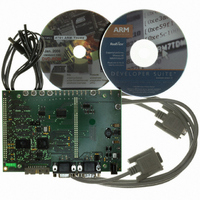
AT91EB40A Atmel, AT91EB40A Datasheet
AT91EB40A
Specifications of AT91EB40A


Related parts for AT91EB40A


AT91EB40A Summary of contents
Page 1
... AT91EB40A Evaluation Board .............................................................................................. User Guide ...
Page 2
...
Page 3
... Table of Contents Section 1 Overview............................................................................................... 1-1 1.1 Scope ........................................................................................................1-1 1.2 Deliverables ..............................................................................................1-1 1.3 The AT91EB40A Evaluation Board...........................................................1-2 Section 2 Setting Up the AT91EB40A Evaluation Board...................................... 2-1 2.1 Electrostatic Warning ................................................................................2-1 2.2 Requirements............................................................................................2-1 2.3 Layout .......................................................................................................2-1 2.4 Jumper Settings ........................................................................................2-2 2.5 Powering Up the Board .............................................................................2-2 2 ...
Page 4
... Section 6 Appendix B – Schematics..................................................................... 6-1 6.1 Schematics ...............................................................................................6-1 Section 7 Appendix C – Bill of Materials............................................................... 7-1 Section 8 Appendix D – Flash Memory Mapping.................................................. 8-1 AT91EB40A Evaluation Board User Guide ...
Page 5
... AT91EB40A Evaluation Board User Guide The AT91EB40A Evaluation Board enables real-time code development and evaluation. It supports the AT91R40008. This guide focuses on the AT91EB40A Evaluation Board as an evaluation and demon- stration platform: ! Section 1 provides an overview. ! Section 2 describes how to set up the evaluation board. ...
Page 6
... Flash (of which 1M byte is available for user software footprint of an extra Flash memory ! 2 x 32-pin EBI expansion connectors ! 2 x 32-pin I/O expansion connectors ! 20-pin JTAG interface connector If required, user-defined peripherals can also be added to the board. See Section 5 for details. AT91EB40A Evaluation Board User Guide ...
Page 7
... Figure 1-1. AT91EB40A Evaluation Board Block Diagram Reset Controller ARM7TDMI Processor JTAG ICE Connector 66 MHz Clock Crystal Generator Interrupt Push-buttons Controller PIO Power Supply VDDCORE (1.8V) VDDIO (3.3V) Note: No external SRAM is fitted on the board. See section “Memories” on page 4-1 for more details. ...
Page 8
... AT91EB40A Evaluation Board User Guide ...
Page 9
... A grounding strap or similar protective device should be worn when handling the board. Avoid touching the compo- nent pins or any other metallic element. In order to set up the AT91EB40A evaluation board, the following requirements are needed: ! The AT91EB40A evaluation board itself. ...
Page 10
... JP5A/JP5B (V ture enables the current consumption of the AT91 product to be measured. See “Power Consumption Measurement Straps (JP5A/B, JP7A/B)” on page 5-3 in Sec- tion 5 for further details. ) and JP7A/JP7B (V ). This fea- DDIO DDCORE AT91EB40A Evaluation Board User Guide ...
Page 11
... AT91EB40A Evaluation Board AT91EB40A Evaluation Board User Guide To test the AT91EB40A Evaluation Board, perform the following procedure: 1. Hold down the SW1 button and power-up the board, or generate a reset and wait for the light sequence on each LED to complete. All the LEDs light. ...
Page 12
... AT91EB40A Evaluation Board User Guide ...
Page 13
... Evaluation Board 3.2 Boot Software Program AT91EB40A Evaluation Board User Guide The AT91EB40A Evaluation Board embeds an AT49BV1604 or AT49BV1614 Flash memory device programmed with default software. When delivered, the Flash memory device contains: ! the Boot Software Program ! the Functional Test Software (FTS) ...
Page 14
... The procedure is as follows: (1) 1. Connect the Serial A ( port of the AT91EB40A Evaluation Board to a host PC Serial Port using the straight serial cable provided. 2. Start the AT91Loader.exe program available in the AT91 Library on the host com- puter. The AT91 Loader must be configured beforehand. For more details, see the documentation regarding the free Host Loader available for download on the Atmel web site ...
Page 15
... SRAM used by Angel is from 0x00020000 to 0x0003FFFF, i.e., the highest half part of the internal SRAM. The Angel on the AT91EB40A Evaluation Board can be upgraded regardless of the ver- sion programmed on it. Note that if the debugger is started through ICE while the Angel monitor is on, the Advanced Interrupt Controller (AIC) and the USART channel are enabled ...
Page 16
... AT91EB40A Evaluation Board User Guide ...
Page 17
... The connector fitted at the factory connector on a 0.1” (2.54 mm) pitch. The schematic (Figure 6-2 on page 6-3 in Section 6, “Appendix B – Schematics”) shows two 128K/512K x 8 SRAM devices that can be added to the AT91EB40A. Note: The AT91EB40A evaluation board does not feature any external SRAM. The user can add SRAM ranging in size from 256K bytes x 16 bits to 1M byte x 16 bits. See “ ...
Page 18
... This device also generates the reset signal in case of watchdog timeout, as the pin NWDOVF of the AT91R40008 is connected on its input /MR. The assertion of this reset signal lights the red RESET LED (D10). By pressing the CLEAR RESET push button (S2), the LED is turned off. AT91EB40A Evaluation Board User Guide ...
Page 19
... JTAG Interface 4.7 Layout Drawing AT91EB40A Evaluation Board User Guide An ARM-standard 20-pin box header (P5) is provided to enable connection of an ICE to the JTAG inputs on the AT91. This allows code to be debugged on the board without using system resources, such as memory and serial ports. ...
Page 20
... AT91EB40A Evaluation Board User Guide ...
Page 21
... Configuration Straps AT91EB40A Evaluation Board User Guide Appendix A – Configuration Straps By using the I/O and EBI expansion connectors, users can connect their own peripher- als to the evaluation board. These peripherals may require more I/O lines than available while the board is in its default state. Extra I/O lines can be made available by disabling some of the on-board peripherals or features ...
Page 22
... The on-board reset signal is not connected to the Flash NRESET input. CB15 Flash RDY/BUSY Pin (U1B) (1) Closed The RDY/BUSY line of the Flash memory is connected to P10/IRQ1 pin. Open The RDY/BUSY line of the Flash memory is not connected to P10/IRQ1 pin. AT91EB40A Evaluation Board User Guide ...
Page 23
... Power Consumption Measurement Straps (JP5A/B, JP7A/B) 5.3 Ground Links (JP6) AT91EB40A Evaluation Board User Guide CB16 Highest Address Bit (1) Open Setting to support an AT49BV1604 or AT49BV1614 (or an AT49BV161) on U1A footprint or an AT49BV8011 (or an AT49BV400) on U1B footprint. Closed Setting to support an AT49BV1604/A on U1A footprint. ...
Page 24
... Memory Size 5-4 2635C–ATARM–13-May-05 The AT91EB40A Evaluation Board is not supplied with external SRAM devices. If, how- ever, the user needs more than 256K bytes of internal memory embedded in the AT91R40008, SRAM from 256K bytes to 1M bytes may be added. The following references for the 128K x 8 SRAM are available: ...
Page 25
... Schematics AT91EB40A Evaluation Board User Guide Appendix B – Schematics The following schematics are appended: ! Figure 6-1. PCB Layout ! Figure 6-2. SRAM Memory Devices and Two-wire Interface Memory ! Figure 6-3. Push Buttons, LEDs and Serial Interface ! Figure 6-4. Reset and JTAG Interface ! Figure 6-5 ...
Page 26
... Figure 6-1. PCB Layout 6-2 2635C–ATARM–13-May-05 AT91EB40A Evaluation Board User Guide ...
Page 27
... Figure 6-2. SRAM Memory Devices and Two-wire Interface Memory AT91EB40A Evaluation Board User Guide 6-3 2635C–ATARM–13-May-05 ...
Page 28
... Figure 6-3. Push Buttons, LEDs and Serial Interface 6-4 2635C–ATARM–13-May-05 AT91EB40A Evaluation Board User Guide ...
Page 29
... Figure 6-4. Reset and JTAG Interfaces AT91EB40A Evaluation Board User Guide 6-5 2635C–ATARM–13-May-05 ...
Page 30
... Figure 6-5. AT91R40008 6-6 2635C–ATARM–13-May-05 AT91EB40A Evaluation Board User Guide ...
Page 31
... Figure 6-6. I/O and EBI Expansion Connectors AT91EB40A Evaluation Board User Guide 6-7 2635C–ATARM–13-May-05 ...
Page 32
... Figure 6-7. Power Supply 6-8 2635C–ATARM–13-May-05 AT91EB40A Evaluation Board User Guide ...
Page 33
... Figure 6-8. Flash Memory Devices AT91EB40A Evaluation Board User Guide 6-9 2635C–ATARM–13-May-05 ...
Page 34
... AT91EB40A Evaluation Board User Guide ...
Page 35
... Table 7-1. Bill of Materials for AT91EB40A Item Qty Reference R13, R23, R24, R104, R105, R107, R108 R5, R14 to R17, R22, R25, R31, R42 to R45, R51, R54, R101 to R103, R106, R109 to R115 3 4 R1, R2, R18, R100 4 6 C78 to C81, C84, C85 5 8 C20, C21, C23, C24, C26, ...
Page 36
... Table 7-1. Bill of Materials for AT91EB40A (Continued) Item Qty Reference TP1, TP2, TP3, TP4 D16 to D19 30 1 D15 31 1 D12 32 1 D14 D8, D10, D11 D22, D23 35 2 D20, D21 SW1 to SW5 U16 45 2 U1A U2 U11 49 1 U19 50 1 U10 51 1 U17 ...
Page 37
... AT91EB40A Evaluation Board User Guide Figure 8-1 shows the embedded software mapping after the remap. It describes the location of the different programs in the AT49BV162A Flash memory and the division into sectors. Figure 8-1. EB40A Flash Memory Software Mapping 0x011FFFFF Not Used LED Swing Application ...
Page 38
... AT91EB40A Evaluation Board User Guide ...
Page 39
... Section 5.1 Figure 6-2 Figure 6-8 Appendix C Appendix D Figure 8-1 2635C–ATARM–13-May-05 AT91EB40A Evaluation Board User Guide 2635 Publication Date: Mar-02 Publication Date: 21-Jun-02 Change in compilation address in SRAM Downloader Publication Date: 13-May-05 Removed "64K bytes of EEPROM" Removed the Two-wire Interface" box Removed " ...
Page 40
... Disclaimer: The information in this document is provided in connection with Atmel products. No license, express or implied, by estoppel or otherwise, to any intellectual property right is granted by this document or in connection with the sale of Atmel products. EXCEPT AS SET FORTH IN ATMEL’S TERMS AND CONDI- TIONS OF SALE LOCATED ON ATMEL’S WEB SITE, ATMEL ASSUMES NO LIABILITY WHATSOEVER AND DISCLAIMS ANY EXPRESS, IMPLIED OR STATUTORY WARRANTY RELATING TO ITS PRODUCTS INCLUDING, BUT NOT LIMITED TO, THE IMPLIED WARRANTY OF MERCHANTABILITY, FITNESS FOR A PARTICULAR PURPOSE, OR NON-INFRINGEMENT ...