MCP9800DM-PCTL Microchip Technology, MCP9800DM-PCTL Datasheet - Page 9
MCP9800DM-PCTL
Manufacturer Part Number
MCP9800DM-PCTL
Description
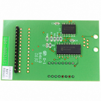
BOARD DEMO FOR PICTAIL MCP9800
Manufacturer
Microchip Technology
Series
PICtail™r
Datasheets
1.MCP9800A0T-MOT.pdf
(42 pages)
2.MCP9800A0T-MOT.pdf
(4 pages)
3.MCP9800DM-PCTL.pdf
(26 pages)
4.MCP9800DM-DL.pdf
(12 pages)
Specifications of MCP9800DM-PCTL
Sensor Type
Temperature
Sensing Range
-55°C ~ 125°C
Interface
I²C, SMBus
Sensitivity
±0.5°C
Voltage - Supply
2.7 V ~ 5.5 V
Embedded
Yes, MCU, 8-Bit
Utilized Ic / Part
MCP9800
Processor To Be Evaluated
MCP9800 and PIC16F684
Data Bus Width
8 bit
Silicon Manufacturer
Microchip
Silicon Core Number
MCP9800
Kit Application Type
Sensing - Temperature
Application Sub Type
Temperature Sensor
Silicon Family Name
PICtail
Kit Contents
Board
Rohs Compliant
Yes
Lead Free Status / RoHS Status
Contains lead / RoHS non-compliant
Lead Free Status / RoHS Status
Lead free / RoHS Compliant, Contains lead / RoHS non-compliant


3.0
The descriptions of the pins are listed in
TABLE 3-1:
3.1
The SDA is a bidirectional input/output pin, used to
serially transmit data to and from the host controller.
This pin requires a pull-up resistor to output data.
3.2
The SCLK is a clock input pin. All communication and
timing is relative to the signal on this pin. The clock is
generated by the host controller on the bus.
3.3
The V
specified in the DC electrical specification table, is
applied on this pin.
3.4
The GND pin is the system ground pin.
2010 Microchip Technology Inc.
MCP9800
MCP9802
SOT-23-5
DD
PIN DESCRIPTION
Serial Data Pin (SDA)
Serial Clock Pin (SCLK)
Power Supply Input (V
pin is the power pin. The operating voltage, as
Ground (GND)
—
—
—
5
4
3
2
1
PIN FUNCTION TABLE
MSOP, SOIC
MCP9801
MCP9803
1
2
3
4
5
6
7
8
DD
Table
)
3-1.
Symbol
ALERT
SCLK
GND
SDA
V
A2
A1
A0
DD
Bidirectional Serial Data
Serial Clock Input
Temperature Alert Output
Ground
Address Select Pin (bit 2)
Address Select Pin (bit 1)
Address Select Pin (bit 0)
Power Supply Input
3.5
The MCP9800/1/2/3’s ALERT pin is an open-drain
output pin. The device outputs an alert signal when the
ambient
user-programmed temperature limit.
3.6
These pins are device or slave address input pins and
are available only with the MCP9801/03. The device
addresses for the MCP9800/02 are factory-set.
The address pins are the Least Significant bits (LSb) of
the device address bits. The Most Significant bits
(MSb) (A6, A5, A4, A3) are factory-set to <1001>. This
is illustrated in
TABLE 3-2:
MCP9800/02A2
MCP9800/02A3
MCP9800/02A4
MCP9800/02A5
MCP9800/02A6
MCP9800/02A7
MCP9801/03
MCP9800/02A0
MCP9800/02A1
Note:
Device
ALERT Output
Address Pins (A2, A1, A0)
User-selectable address is shown by X.
temperature
Table
MCP9800/1/2/3
SLAVE ADDRESS
A6
1
1
1
1
1
1
1
1
1
3-2.
Function
A5
0
0
0
0
0
0
0
0
0
A4
goes
0
0
0
0
0
0
0
0
0
A3
1
1
1
1
1
1
1
1
1
DS21909D-page 9
beyond
A2
0
0
0
0
1
1
1
1
X
A1
0
0
1
1
0
0
1
1
X
A0
0
1
0
1
0
1
0
1
X
the
Related parts for MCP9800DM-PCTL
Image
Part Number
Description
Manufacturer
Datasheet
Request
R

Part Number:
Description:
DEMO BOARD TEMP SENSOR MCP9800
Manufacturer:
Microchip Technology
Datasheet:

Part Number:
Description:
BOARD DEMO 2 FOR MCP9800
Manufacturer:
Microchip Technology
Datasheet:

Part Number:
Description:
BOARD DEMO FOR MCP9800
Manufacturer:
Microchip Technology
Datasheet:

Part Number:
Description:
Manufacturer:
Microchip Technology Inc.
Datasheet:
Part Number:
Description:
Manufacturer:
Microchip Technology Inc.
Datasheet:
Part Number:
Description:
Manufacturer:
Microchip Technology Inc.
Datasheet:
Part Number:
Description:
Manufacturer:
Microchip Technology Inc.
Datasheet:
Part Number:
Description:
Manufacturer:
Microchip Technology Inc.
Datasheet:
Part Number:
Description:
Manufacturer:
Microchip Technology Inc.
Datasheet:
Part Number:
Description:
Manufacturer:
Microchip Technology Inc.
Datasheet: